DLPS023C January 2012 – August 2015 DLPC300
PRODUCTION DATA.
- 1 Features
- 2 Applications
- 3 Description
- 4 Revision History
- 5 Pin Configuration and Functions
-
6 Specifications
- 6.1 Absolute Maximum Ratings
- 6.2 ESD Ratings
- 6.3 Recommended Operating Conditions
- 6.4 Thermal Information
- 6.5 I/O Electrical Characteristics
- 6.6 Crystal Port Electrical Characteristics
- 6.7 Power Consumption
- 6.8 I2C Interface Timing Requirements
- 6.9 Parallel Interface Frame Timing Requirements
- 6.10 Parallel Interface General Timing Requirements
- 6.11 Parallel I/F Maximum Supported Horizontal Line Rate
- 6.12 BT.565 I/F General Timing Requirements
- 6.13 Flash Interface Timing Requirements
- 6.14 DMD Interface Timing Requirements
- 6.15 Mobile Dual Data Rate (mDDR) Memory Interface Timing Requirements
- 6.16 JTAG Interface: I/O Boundary Scan Application Switching Characteristics
- 7 Detailed Description
-
8 Application and Implementation
- 8.1 Application Information
- 8.2 Typical Application
- 8.3 System Examples
- 9 Power Supply Recommendations
-
10Layout
- 10.1
Layout Guidelines
- 10.1.1 Printed Circuit Board Design Guidelines
- 10.1.2 Printed Circuit Board Layer Stackup Geometry
- 10.1.3 Signal Layers
- 10.1.4 Routing Constraints
- 10.1.5 Termination Requirements
- 10.1.6 PLL
- 10.1.7 General Handling Guidelines for Unused CMOS-Type Pins
- 10.1.8 Hot-Plug Usage
- 10.1.9 External Clock Input Crystal Oscillator
- 10.2 Layout Example
- 10.3 Thermal Considerations
- 10.1
Layout Guidelines
- 11Device and Documentation Support
- 12Mechanical, Packaging, and Orderable Information
Package Options
Refer to the PDF data sheet for device specific package drawings
Mechanical Data (Package|Pins)
- ZVB|176
Thermal pad, mechanical data (Package|Pins)
Orderable Information
9 Power Supply Recommendations
9.1 System Power-Up and Power-Down Sequence
Although the DLPC300 requires an array of power supply voltages, (for example, VDD, VDD_PLL, VCC_18, VCC_FLSH, VCC_INTF), there are no restrictions regarding the relative order of power supply sequencing to avoid damaging the DLPC300. This is true for both power-up and power-down scenarios. Similarly, there is no minimum time between powering up or powering down the different supplies feeding the DLPC300. Note, however, that it is not uncommon for there to be power-sequencing requirements for the devices that share the supplies with the DLPC300.
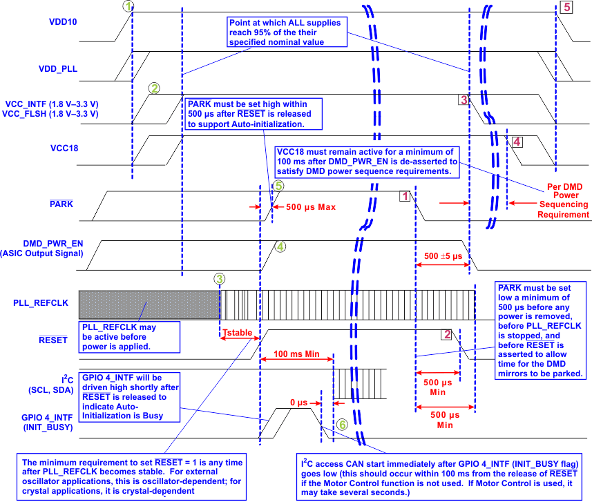
Although there is no risk of damaging the DLPC300 as a result of a given power sequence, from a functional standpoint, there is one specific power-sequencing recommendation to ensure proper operation. In particular, all controller power should be applied and allowed to reach minimum specified voltage levels before RESET is deasserted to ensure proper power-up initialization is performed. All I/O power should remain applied as long as 1-V core power is applied and RESET is deasserted.
Note that when VDD10 core power is applied but I/O power is not applied, additional leakage current may be drawn.
 Figure 17. Power-Up/Down Timing
9.1.1 Power Up Sequence
To minimize leakage currents and ensure proper operation, apply the following power up sequence. These steps are numbered in green with a circle around the step number in Figure 17.
- Apply power to VDD10 and VDD_PLL while driving RESET low
- After VDD10 power has reached minimum operating voltage, apply power to VCC18, VCC_INTF, and VCC_FLSH
- After VCC18, VCC_INTF, and VCC_FLSH have reached minimum operating voltage, wait for the reference clock to stabilize (PLL_REFCLK). The time for the clock to stabilize depend on the external crystal or oscillator. Refer to the corresponding crystal or oscillator data sheet for appropriate time
- Once the reference clock is stable, release reset to DLPC300 by driving RESET high. GPIO4_INTF will be driven high by the DLPC300 to indicate that Auto-Initialization is Busy
- Drive PARK high within 500usec after RESET is driven high
- Wait for DLPC300 to drive GPIO4_INTF low ( a minimum of 100 ms) to indicate that the DLPC300 has completed the auto-Initialization and the device is ready to accept I2C commands
9.1.2 Power Down Sequence
To minimize leakage currents and ensure proper operation, apply the following power down sequence. These steps are numbered in red with a square around the step number in Figure 17.
- Drive PARK low. This starts the park sequence which takes a maximum of 500 usec
- Wait a minimum of 500 usec after driving PARK low before driving RESET low
- Wait for DLPC300 to drive DMD_PWR_EN low before removing power to VCC_INTF and VCC_FLSH
- Wait a minimum of 100 ms after DLPC300 drives DMD_PWR_EN low before removing power to VCC18
- Once power has been removed from VCC18, remove power to VDD10 and VDD_PLL
9.1.3 Additional Power-Up Initialization Sequence Details
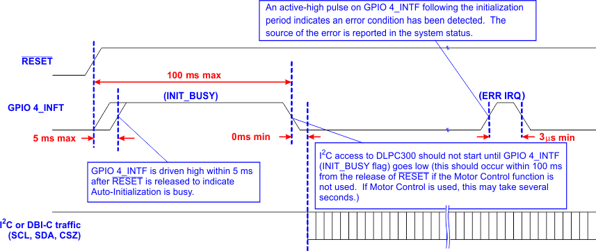
It is assumed that an external power monitor holds the DLPC300 in system reset during power-up. It must do this by driving RESET to a logic-low state. It should continue to assert system reset until all controller voltages have reached minimum specified voltage levels, PARK is asserted high, and input clocks are stable. During this time, most controller outputs are driven to an inactive state and all bidirectional signals are configured as inputs to avoid contention. Controller outputs that are not driven to an inactive state are in the high-impedance state. These include DMD_PWR_EN, LEDDVR_ON, LED_SEL_0, LED_SEL_1, SPICLK, SPIDOUT, and SPICS0. After power is stable and the PLL_REFCLK clock input to the DLPC300 is stable, then RESET should be deactivated (set to a logic high). The DLPC300 then performs a power-up initialization routine that first locks its PLL followed by loading self-configuration data from the external flash. On release of RESET, all DLPC300 I/Os become active. Immediately following the release of RESET, the INIT_BUSY signal is driven high to indicate that the auto-initialization routine is in progress. On completion of the auto-initialization routine, the DLPC300 drives INIT_BUSY low to signal INITIALIZATION DONE.
Note that the host processor can start sending standard I2C commands after INIT_BUSY goes low, or a 100-ms timer expires in the host processor, whichever is earlier.
See Figure 18 for a visualization of this sequence.
 Figure 18. Initialization Timeline
9.2 System Power I/O State Considerations
Note that:
- If VCC18 I/O power is applied when VDD10 core power is not applied, then all mDDR (non fail-safe) and non-mDDR (fail-safe) output signals associated with the VCC18 supply are in a high-impedance state.
- If VCC_INTF or VCC_FLSH I/O power is applied when VDD10 core power is not applied, then all output signals associated with these inactive I/O supplies are in a high-impedance state.
- If VDD10 core power is applied but VCC_INTF or VCC_FLSH I/O power is not applied, then all output signals associated with these inactive I/O supplies are in a high-impedance state.
- If VDD10 core power is applied but VCC18 I/O power is not applied, then all mDDR (non fail-safe) and non-mDDR (fail-safe) output signals associated with the VCC18 I/O supply are in a high-impedance state; however, if driven high externally, only the non-mDDR (fail-safe) output signals remain in a high-impedance state, and the mDDR (non fail-safe) signals are shorted to ground through clamping diodes.
9.3 Power-Good (PARK) Support
The PARK signal is defined to be an early warning signal that should alert the controller 500 µs before dc supply voltages have dropped below specifications. This allows the controller time to park the DMD, ensuring the integrity of future operation. Note that the reference clock should continue to run and RESET should remain deactivated for at least 500 µs after PARK has been deactivated (set to a logic low) to allow the park operation to complete.