SNLS266E May 2007 – March 2015 DP83848C , DP83848I , DP83848VYB , DP83848YB
PRODUCTION DATA.
- 1Introduction
- 2Revision History
- 3 Device Comparison
-
4Pin Configuration and Functions
- 4.1 Pin Layout
- 4.2 Package Pin Assignments
- 4.3 Serial Management Interface
- 4.4 Mac Data Interface
- 4.5 Clock Interface
- 4.6 LED Interface
- 4.7 JTAG Interface for DP83848I/VYB/YB
- 4.8 Reset and Power Down
- 4.9 Strap Options
- 4.10 10 Mb/s and 100 Mb/s PMD Interface
- 4.11 Special Connections
- 4.12 Power Supply Pins
- 5Specifications
-
6Detailed Description
- 6.1 Overview
- 6.2 Functional Block Diagram
- 6.3 Feature Description
- 6.4 Device Functional Modes
- 6.5
Programming
- 6.5.1
Architecture
- 6.5.1.1 100BASE-TX Transmitter
- 6.5.1.2
100BASE-TX Receiver
- 6.5.1.2.1 Analog Front End
- 6.5.1.2.2 Digital Signal Processor
- 6.5.1.2.3 Signal Detect
- 6.5.1.2.4 MLT-3 to NRZI Decoder
- 6.5.1.2.5 NRZI to NRZ
- 6.5.1.2.6 Serial to Parallel
- 6.5.1.2.7 Descrambler
- 6.5.1.2.8 Code-group Alignment
- 6.5.1.2.9 4B/5B Decoder
- 6.5.1.2.10 100BASE-TX Link Integrity Monitor
- 6.5.1.2.11 Bad SSD Detection
- 6.5.1.3
10BASE-T Transceiver Module
- 6.5.1.3.1 Operational Modes
- 6.5.1.3.2 Smart Squelch
- 6.5.1.3.3 Collision Detection and SQE
- 6.5.1.3.4 Carrier Sense
- 6.5.1.3.5 Normal Link Pulse Detection/Generation
- 6.5.1.3.6 Jabber Function
- 6.5.1.3.7 Automatic Link Polarity Detection and Correction
- 6.5.1.3.8 Transmit and Receive Filtering
- 6.5.1.3.9 Transmitter
- 6.5.1.3.10 Receiver
- 6.5.1
Architecture
- 6.6
Memory
- 6.6.1
Register Block
- 6.6.1.1
Register Definition
- 6.6.1.1.1 Basic Mode Control Register (BMCR)
- 6.6.1.1.2 Basic Mode Status Register (BMSR)
- 6.6.1.1.3 PHY Identifier Register #1 (PHYIDR1)
- 6.6.1.1.4 PHY Identifier Register #2 (PHYIDR2)
- 6.6.1.1.5 Auto-Negotiation Advertisement Register (ANAR)
- 6.6.1.1.6 Auto-Negotiation Link Partner Ability Register (ANLPAR) (BASE Page)
- 6.6.1.1.7 Auto-Negotiation Link Partner Ability Register (ANLPAR) (Next Page)
- 6.6.1.1.8 Auto-Negotiate Expansion Register (ANER)
- 6.6.1.1.9 Auto-Negotiation Next Page Transmit Register (ANNPTR)
- 6.6.1.2
Extended Registers
- 6.6.1.2.1 PHY Status Register (PHYSTS)
- 6.6.1.2.2 MII Interrupt Control Register (MICR)
- 6.6.1.2.3 MII Interrupt Status and Misc. Control Register (MISR)
- 6.6.1.2.4 False Carrier Sense Counter Register (FCSCR)
- 6.6.1.2.5 Receiver Error Counter Register (RECR)
- 6.6.1.2.6 100 Mb/s PCS Configuration and Status Register (PCSR)
- 6.6.1.2.7 RMII and Bypass Register (RBR)
- 6.6.1.2.8 LED Direct Control Register (LEDCR)
- 6.6.1.2.9 PHY Control Register (PHYCR)
- 6.6.1.2.10 10 Base-T Status/Control Register (10BTSCR)
- 6.6.1.2.11 CD Test and BIST Extensions Register (CDCTRL1)
- 6.6.1.2.12 Energy Detect Control (EDCR)
- 6.6.1.1
Register Definition
- 6.6.1
Register Block
- 7Application, Implementation, and Layout
- 8Device and Documentation Support
- 9Mechanical, Packaging, and Orderable Information
Package Options
Mechanical Data (Package|Pins)
- PT|48
Thermal pad, mechanical data (Package|Pins)
Orderable Information
1 Introduction
1.1 Features
- Multiple Temperature Range from –40°C to 105°C
- Low-Power 3.3-V, 0.18-µm CMOS Technology
- Low-Power Consumption < 270 mW Typical
- 3.3-V MAC Interface
- Auto-MDIX for 10/100 Mb/s
- Energy Detection Mode
- 25-MHz Clock Output
- SNI Interface (Configurable)
- RMII Rev. 1.2 Interface (Configurable)
- MII Serial Management Interface (MDC and MDIO)
- IEEE 802.3 MII
- IEEE 802.3 Auto-Negotiation and Parallel Detection
- IEEE 802.3 ENDEC, 10BASE-T Transceivers and Filters
- IEEE 802.3 PCS, 100BASE-TX Transceivers and Filters
- IEEE 1149.1 JTAG
- Integrated ANSI X3.263 Compliant TP-PMD Physical Sub-Layer with Adaptive Equalization and Baseline Wander Compensation
- Error-Free Operation up to 150 Meters
- Programmable LED Support for Link, 10/100 Mb/s Mode, Activity, Duplex and Collision Detect
- Single Register Access for Complete PHY Status
- 10/100 Mb/s Packet BIST (Built in Self Test)
1.2 Applications
- Automotive/Transportation
- Industrial Controls and Factory Automation
- General Embedded Applications
1.3 Description
The number of applications requiring Ethernet connectivity continues to increase, driving Ethernet enabled devices into harsher environments.
The DP83848C/I/VYB/YB was designed to meet the challenge of these new applications with an extended temperature performance that goes beyond the typical Industrial temperature range. The DP83848C/I/VYB/YB is a highly reliable, feature rich, robust device which meets IEEE 802.3 standards over multiple temperature ranges from commercial to extreme temperatures. This device is ideally suited for harsh environments such as wireless remote base stations, automotive/transportation, and industrial control applications.
It offers enhanced ESD protection and the choice of an MII or RMII interface for maximum flexibility in MPU selection; all in a 48 pin package.
The DP83848VYB extends the leadership position of the PHYTER™ family of devices with a wide operating temperature range. The TI line of PHYTER transceivers builds on decades of Ethernet expertise to offer the high performance and flexibility that allows the end user an easy implementation tailored to meet these application needs.
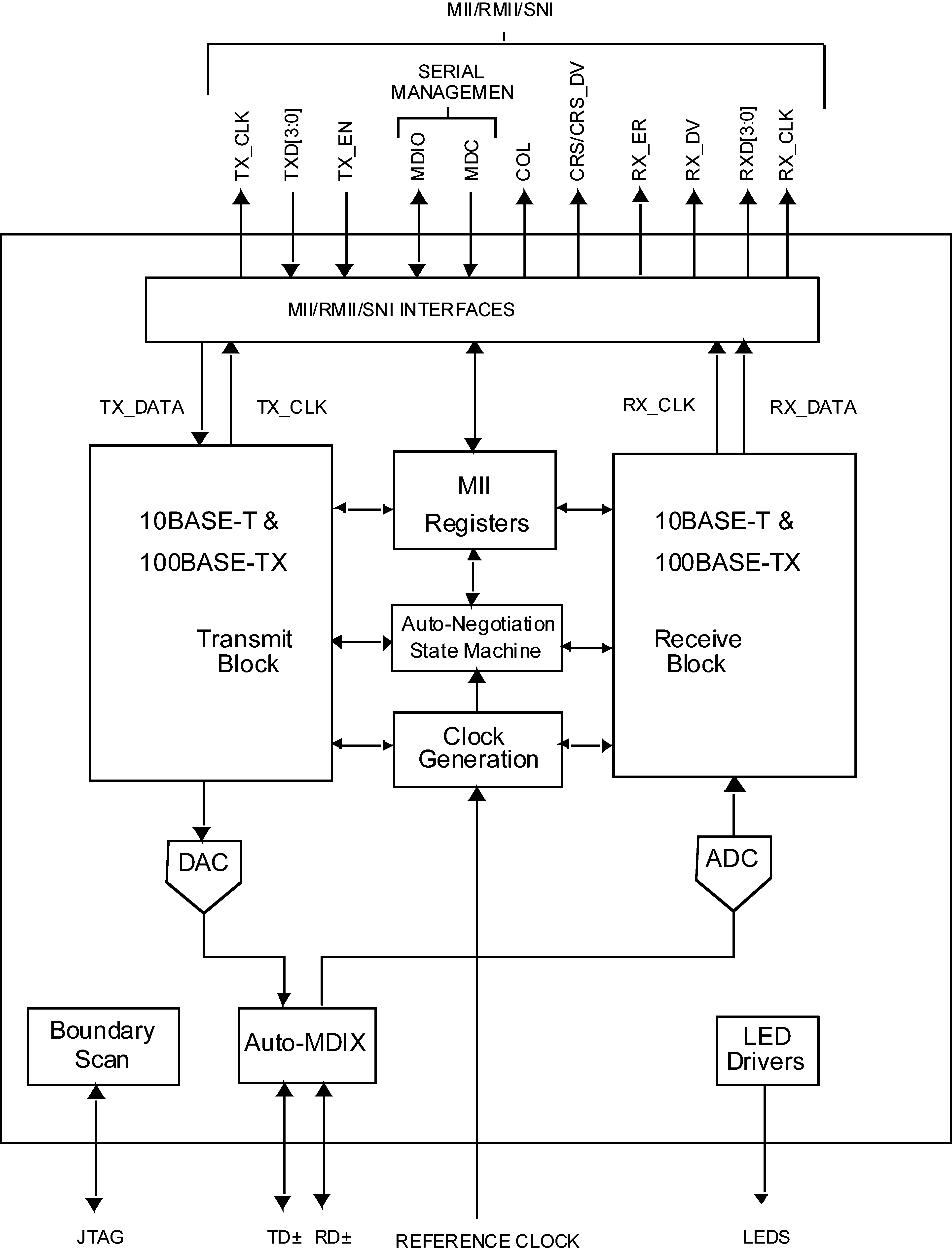
1.4 Functional Block Diagram
