SBOS094B January 1998 – December 2014 DRV134 , DRV135
PRODUCTION DATA.
- 1 Features
- 2 Applications
- 3 Description
- 4 Simplified Schematic
- 5 Revision History
- 6 Pin Configuration and Functions
- 7 Specifications
- 8 Detailed Description
- 9 Application and Implementation
- 10Power Supply Recommendations
- 11Layout
- 12Device and Documentation Support
- 13Mechanical, Packaging, and Orderable Information
Package Options
Mechanical Data (Package|Pins)
Thermal pad, mechanical data (Package|Pins)
- DW|16
Orderable Information
7 Specifications
7.1 Absolute Maximum Ratings
over operating free-air temperature range (unless otherwise noted) (1)| MIN | MAX | UNIT | ||
|---|---|---|---|---|
| Supply voltage, V+ to V– | 40 | V | ||
| Input voltage range | V– | V+ | ||
| Output short-circuit (to ground) | Continuous | |||
| Operating temperature | –55 | 125 | °C | |
| Junction temperature | 150 | °C |
(1) Stresses beyond those listed under Absolute Maximum Ratings may cause permanent damage to the device. These are stress ratings only, which do not imply functional operation of the device at these or any other conditions beyond those indicated under Recommended Operating Conditions. Exposure to absolute-maximum-rated conditions for extended periods may affect device reliability.
7.2 Handling Ratings
| MIN | MAX | UNIT | |||
|---|---|---|---|---|---|
| Tstg | Storage temperature range | –55 | 125 | °C | |
| V(ESD) | Electrostatic discharge | Human body model (HBM), per ANSI/ESDA/JEDEC JS-001, all pins(1) | –2000 | 2000 | V |
| Charged device model (CDM), per JEDEC specification JESD22-C101, all pins(2) | –500 | 500 | |||
(1) JEDEC document JEP155 states that 500-V HBM allows safe manufacturing with a standard ESD control process.
(2) JEDEC document JEP157 states that 250-V CDM allows safe manufacturing with a standard ESD control process.
7.3 Recommended Operating Conditions
over operating free-air temperature range (unless otherwise noted)| MIN | NOM | MAX | UNIT | ||
|---|---|---|---|---|---|
| Tspe | Specification temperature range | –40 | 85 | °C | |
| TA | Operation temperature range | –55 | 125 | °C | |
| V+ | Positive supply | 4.5 | 18 | 18 | V |
| V– | Negative supply | –4.5 | –18 | –18 | V |
7.4 Electrical Characteristics
At TA = +25°C, VS = ±18 V, RL = 600 Ω differential connected between +VO and –VO, unless otherwise noted.| PARAMETER | TEST CONDITIONS | MIN | TYP | MAX | UNIT | |||
|---|---|---|---|---|---|---|---|---|
| AUDIO PERFORMANCE | ||||||||
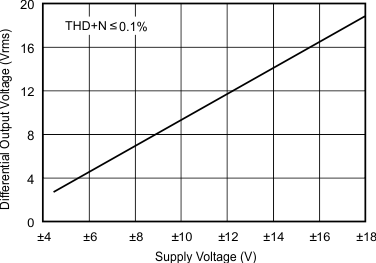
| THD+N | Total Harmonic Distortion + Noise | f = 20Hz to 20kHz, VO = 10Vrms f = 1kHz, VO = 10Vrms 20 kHz BW THD+N < 1% |
0.001% | |||||
| 0.0005% | ||||||||
| RTO(1) | Noise Floor | –98 | dBu | |||||
| RTO(1) | Headroom | 27 | dBu | |||||
| INPUT | ||||||||
| ZIN | Input Impedance(2) | 10 | kΩ | |||||
| IIN | Input Current | VIN = ±7.07 V | –1000 | ±700 | 1000 | µA | ||
| GAIN | ||||||||
| Differential | [(+VO) – (–VO)]/VIN
VIN = ±10V |
|||||||
| Initial | 5.8 | 6 | dB | |||||
| Error | –2% | ±0.1% | 2% | |||||
| Error vs Temperature | ±10 | ppm/°C | ||||||
| Single-Ended | VIN = ±5V | |||||||
| Initial | 5.8 | 6 | dB | |||||
| Error | –2% | ±0.7% | 2% | |||||
| Error vs Temperature | ±10 | ppm/°C | ||||||
| Nonlinearity | 0.0003 | % of FS | ||||||
| OUTPUT | ||||||||
| OCMR | Common-Mode Rejection, f = 1kHz | See Figure 25 | 46 | 68 | dB | |||
| SBR | Signal Balance Ratio, f = 1kHz | See Figure 26 | 35 | 54 | dB | |||
| Output Offset Voltage | ||||||||
| VOCM(3) | Offset Voltage, Common-Mode | VIN = 0 | –250 | ±50 | 250 | mV | ||
| Offset Voltage, Common-Mode vs Temperature | ±150 | µV/°C | ||||||
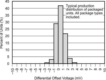
| VOD(4) | Offset Voltage, Differential | VIN = 0 | –10 | ±1 | 10 | mV | ||
| Offset Voltage, Differential vs Temperature | ±5 | µV/°C | ||||||
| PSRR | Offset Voltage, Differential vs Power Supply | VS = ±4.5V to ±18V | 80 | 110 | dB | |||
| Output Voltage Swing, | Positive | No Load(5) | (V+) – 3 | (V+) – 2.5 | V | |||
| Negative | (V–) + 2 | (V–) + 1.5 | ||||||
| Impedance | 50 | Ω | ||||||
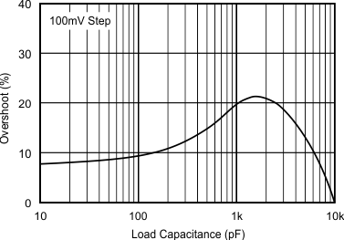
| CL | Load Capacitance, Stable Operation | CL Tied to Ground (each output) | 1 | µF | ||||
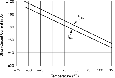
| ISC | Short-Circuit Current | ±85 | mA | |||||
| FREQUENCY RESPONSE | ||||||||
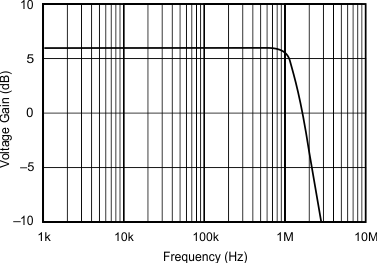
| Small-Signal Bandwidth | 1.5 | MHz | ||||||
| SR | Slew Rate | 15 | V/µs | |||||
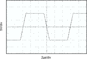
| Settling Time: 0.01% | VOUT = 10V Step | 2.5 | µs | |||||
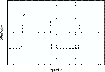
| Overload Recovery | Output Overdriven 10% | 3 | µs | |||||
| POWER SUPPLY | ||||||||
| VS | Rated Voltage | ±18 | V | |||||
| Voltage Range | ±4.5 | ±18 | V | |||||
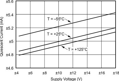
| IQ | Quiescent Current | IO = 0 | –5.5 | ±5.2 | 5.5 | mA | ||
| TEMPERATURE RANGE | ||||||||
| Specification Range | –40 | 85 | °C | |||||
| Operation Range | –55 | 125 | °C | |||||
| Storage Range | –55 | 125 | °C | |||||
| θJA | Thermal Resistance | 8-Pin DIP | 100 | °C/W | ||||
| SO-8 Surface mount | 150 | °C/W | ||||||
| SOL-16 Surface mount | 80 | °C/W | ||||||
(1) dBu = 20log (Vrms /0.7746); RTO = Referred-to-Output.
(2) Resistors are ratio matched but have ±20% absolute value.
(3) VOCM = [(+VO) + (–VO)] / 2.
(4) VOD = (+VO) – (–VO).
(5) Ensures linear operation. Includes common-mode offset.
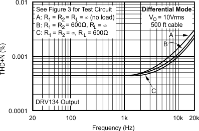
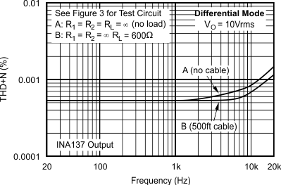
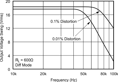
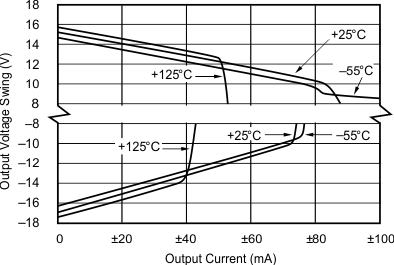
7.5 Typical Characteristics
At TA = 25°C, VS = ±18 V, RL = 600 Ω differential connected between +VO and –VO, unless otherwise noted.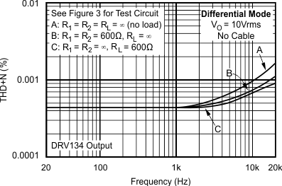
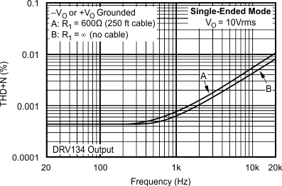
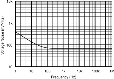
vs Frequency
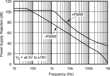
vs Frequency
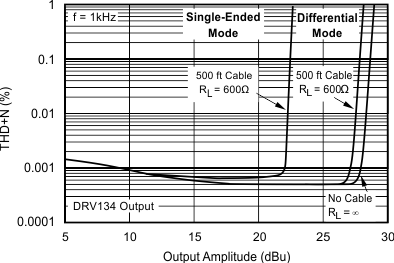
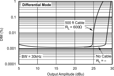
vs Output Amplitude
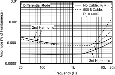
vs Frequency
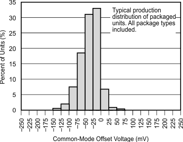
Production Distribution
| CL = 100 pF | ||
| CL = 100 pF | ||
vs Output Amplitude
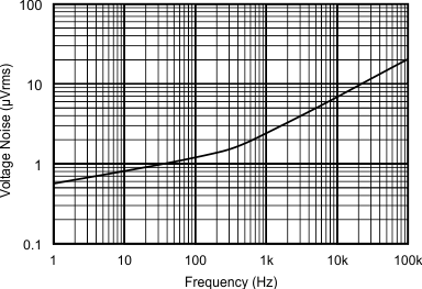
vs Noise Bandwidth
A.
Figure 18. Common-Mode Offset Voltage Production Distribution
| CL = 1000 pF | ||
| CL = 1000 pF | ||