SBOS704B May 2015 – March 2016 DRV421
PRODUCTION DATA.
- 1 Features
- 2 Applications
- 3 Description
- 4 Revision History
- 5 Pin Configuration and Functions
- 6 Specifications
-
7 Detailed Description
- 7.1 Overview
- 7.2 Functional Block Diagram
- 7.3
Feature Description
- 7.3.1 Fluxgate Sensor
- 7.3.2 Integrator-Filter Function and Compensation Loop Stability
- 7.3.3 H-Bridge Driver for Compensation Coil
- 7.3.4 Shunt Sense Amplifier
- 7.3.5 Overrange Comparator
- 7.3.6 Voltage Reference
- 7.3.7 Overload Detection and Control
- 7.3.8 Magnetic Core Demagnetization
- 7.3.9 Search Function
- 7.3.10 Error Flag
- 7.4 Device Functional Modes
- 8 Application and Implementation
- 9 Power-Supply Recommendations
- 10Layout
- 11Device and Documentation Support
- 12Mechanical, Packaging, and Orderable Information
Package Options
Mechanical Data (Package|Pins)
- RTJ|20
Thermal pad, mechanical data (Package|Pins)
- RTJ|20
Orderable Information
6 Specifications
6.1 Absolute Maximum Ratings
over operating free-air temperature range (unless otherwise noted) (1)| MIN | MAX | UNIT | |||
|---|---|---|---|---|---|
| Voltage | Supply voltage (VDD to GND) | –0.3 | 7 | V | |
| Input voltage, except pins AINP and AINN (2) | GND – 0.5 | VDD + 0.5 | |||
| Shunt sense amplifier inputs (pins AINP and AINN) (3) | GND – 6.0 | VDD + 6.0 | |||
| Current | Pins ICOMP1 and ICOMP2 (short circuit current ISC) (4) | –300 | 300 | mA | |
| Shunt sense amplifier inputs | pins AINP and AINN | –5 | 5 | ||
| All remaining pins | –25 | 25 | |||
| Temperature | Junction, TJ max | –50 | 150 | °C | |
| Storage, Tstg | –65 | 150 | |||
(1) Stresses beyond those listed under Absolute Maximum Ratings may cause permanent damage to the device. These are stress ratings only, which do not imply functional operation of the device at these or any other conditions beyond those indicated under Recommended Operating Conditions. Exposure to absolute-maximum-rated conditions for extended periods may affect device reliability.
(2) Input terminals are diode-clamped to the power-supply rails. Input signals that can swing more than 0.5 V beyond the supply rails must be current limited, except for the shunt sense amplifier input pins.
(3) These inputs are not diode-clamped to the power supply rails.
(4) Power-limited; observe maximum junction temperature.
6.2 ESD Ratings
| VALUE | UNIT | |||
|---|---|---|---|---|
| V(ESD) | Electrostatic discharge | Human-body model (HBM), per ANSI/ESDA/JEDEC JS-001(1) | ±2000 | V |
| Charged-device model (CDM), per JEDEC specification JESD22-C101(2) | ±1000 | |||
(1) JEDEC document JEP155 states that 500-V HBM allows safe manufacturing with a standard ESD control process.
(2) JEDEC document JEP157 states that 250-V CDM allows safe manufacturing with a standard ESD control process.
6.3 Recommended Operating Conditions
over operating free-air temperature range (unless otherwise noted)| MIN | NOM | MAX | UNIT | ||
|---|---|---|---|---|---|
| VDD | Supply voltage | 3.0 | 5.0 | 5.5 | V |
| TA | Specified ambient temperature range | –40 | 125 | °C | |
6.4 Thermal Information
| THERMAL METRIC (1) | SBOS704 | UNITS | |
|---|---|---|---|
| RTJ (WQFN) | |||
| 20 PINS | |||
| RθJA | Junction-to-ambient thermal resistance | 34.1 | °C/W |
| RθJC(top) | Junction-to-case (top) thermal resistance | 33.1 | °C/W |
| RθJB | Junction-to-board thermal resistance | 11.0 | °C/W |
| ψJT | Junction-to-top characterization parameter | 0.3 | °C/W |
| ψJB | Junction-to-board characterization parameter | 11.0 | °C/W |
| RθJC(bot) | Junction-to-case (bottom) thermal resistance | 2.1 | °C/W |
(1) For more information about traditional and new thermal metrics, see the Semiconductor and IC Package Thermal Metrics application report, SPRA953.
6.5 Electrical Characteristics
All minimum and maximum specifications at TA = +25°C, VDD = 3.0 V to 5.5 V, and ICOMP1 = ICOMP2 = 0 mA (unless otherwise noted). Typical values are at VDD = 5.0 V.| PARAMETER | TEST CONDITIONS | MIN | TYP | MAX | UNIT | |||
|---|---|---|---|---|---|---|---|---|
| FLUXGATE SENSOR FRONT-END | ||||||||
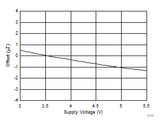
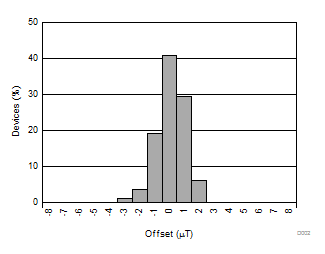
| Offset (1) | No magnetic field | –8 | ±2 | 8 | µT | |||
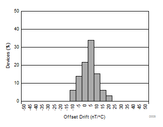
| Offset drift | No magnetic field | ±5 | nT/°C | |||||
| Noise | f = 0.1 Hz to 10 Hz | 17 | nTrms | |||||
| Noise density | f = 1 kHz | 1.5 | nT/√Hz | |||||
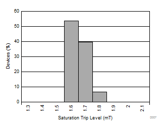
| Saturation trip level for pin ER | 1.7 | mT | ||||||
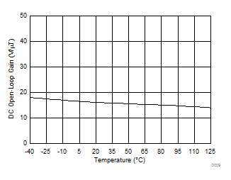
| AOL | DC open-loop gain | 16 | V/µT | |||||
| AC open-loop gain | GSEL[1:0] = 00, at 3.8 kHz, integration-to-flatband corner frequency |
8.5 | V/mT | |||||
| GSEL[1:0] = 01, at 3.8 kHz, integration-to-flatband corner frequency |
38 | |||||||
| GSEL[1:0] = 10, at 1.9 kHz, integration-to-flatband corner frequency |
25 | |||||||
| GSEL[1:0] = 11, at 1.9 kHz, integration-to-flatband corner frequency |
70 | |||||||
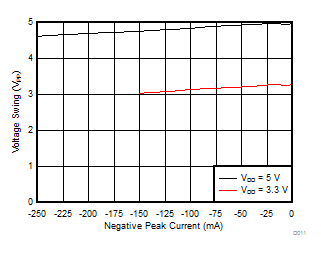
| IICOMP | Peak current at pins ICOMP1 and ICOMP2 | VICOMP1 – VICOMP2 = 4.2 VPP,VDD = 5 V, TA = –40°C to +125°C |
210 | 250 | mA | |||
| VICOMP1 – VICOMP2 = 2.5 VPP, VDD = 3.3 V, TA = –40°C to +125°C |
125 | 150 | ||||||
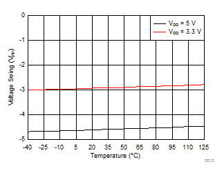
| VICOMP | Voltage swing at pins ICOMP1 and ICOMP2 | 20-Ω load, VDD = 5 V, TA = –40°C to +125°C | 4.2 | VPP | ||||
| 20-Ω load, VDD = 3.3 V, TA = –40°C to +125°C | 2.5 | |||||||
| Common-mode output voltage at pins ICOMP1 and ICOMP2 | VREFOUT | V | ||||||
| SHUNT SENSE AMPLIFIER | ||||||||
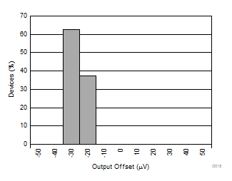
| VOO | Output offset voltage | VAINP = VAINN = VREFIN, VDD = 3.0 V | –0.075 | ±0.01 | 0.075 | mV | ||
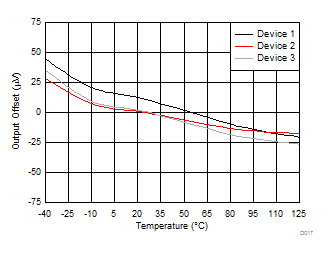
| Output offset voltage drift | –2 | ±0.4 | 2 | µV/°C | ||||
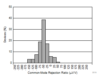
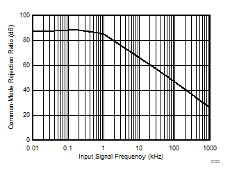
| CMRR | Common-mode rejection ratio, RTO (2) | VCM = −1 V to VDD + 1 V, VREFIN = VDD / 2 | –250 | ±50 | 250 | µV/V | ||
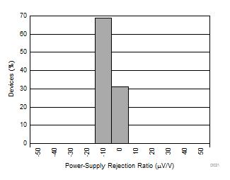
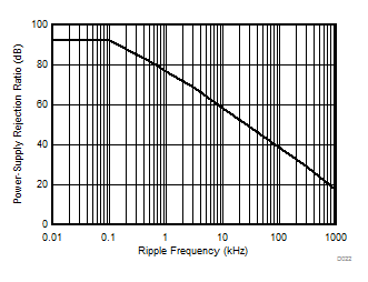
| PSRRAMP | Power-supply rejection ratio, RTO | VDD = 3.0 V to 5.5 V, VCM = VREFIN | –50 | ±4 | 50 | µV/V | ||
| VIC | Common-mode input voltage range | –1 | VDD + 1 | V | ||||
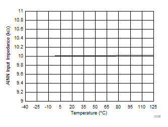
| ZIND | Differential input impedance | 16.5 | 20 | 23.5 | kΩ | |||
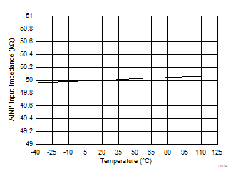
| ZIC | Common-mode input impedance | 40 | 50 | 60 | kΩ | |||
| G | Gain, VOUT / (VAINP – VAINN) | 4 | V/V | |||||
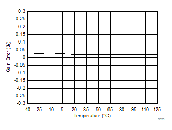
| EG | Gain error | –0.3% | ±0.02% | 0.3% | ||||
| Gain error drift | –5 | ±1 | 5 | ppm/°C | ||||
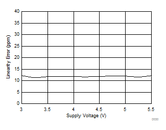
| Linearity error | RL = 1 kΩ | 12 | ppm | |||||
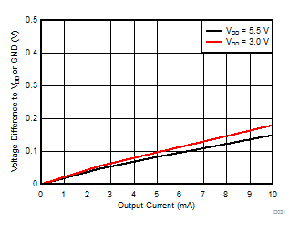
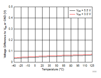
| Voltage output swing from negative rail (OR pin trip level) |
VDD = 5.5 V, IVOUT = 2.5 mA | 48 | 85 | mV | ||||
| VDD = 3.0 V, IVOUT = 2.5 mA | 56 | 100 | ||||||
| Voltage output swing from positive rail (OR pin trip level) |
VDD = 5.5 V, IVOUT = –2.5 mA | VDD – 85 | VDD – 48 | mV | ||||
| VDD = 3.0 V, IVOUT = –2.5 mA | VDD – 100 | VDD – 56 | ||||||
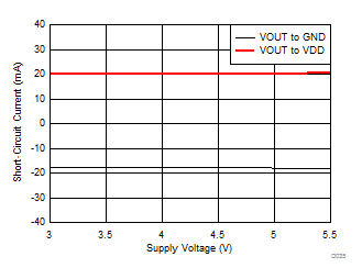
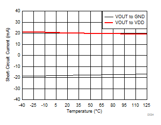
| ISC | Short-circuit current | VOUT connected to GND | –18 | mA | ||||
| VOUT connected to VDD | 20 | |||||||
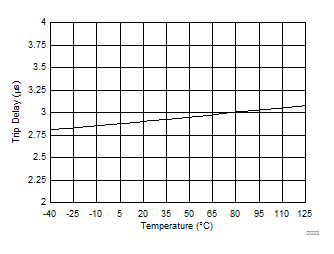
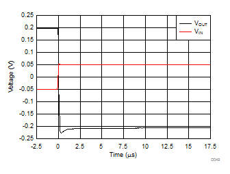
| Signal overrange indication delay (OR pin) | VIN = 1-V step | 2.5 to 3.5 | µs | |||||
| BW–3dB | Bandwidth | 2 | MHz | |||||
| SR | Slew rate | 6.5 | V/µs | |||||
| Settling time, large-signal | ΔV = ± 2 V to 1% accuracy, no external filter | 0.9 | µs | |||||
| Settling time, small-signal | ΔV = ± 0.4 V to 0.01% accuracy | 8 | µs | |||||
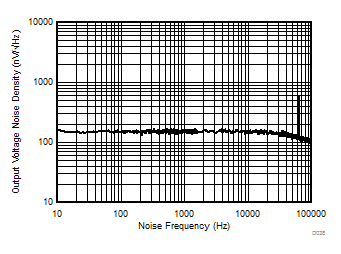
| en | Output voltage noise density, RTO | f = 1 kHz, compensation loop disabled | 170 | nV/√Hz | ||||
| VREFIN | Input voltage range at pin REFIN | TA = –40°C to +125°C | GND | VDD | V | |||
| VOLTAGE REFERENCE | ||||||||
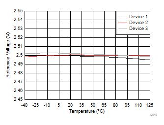
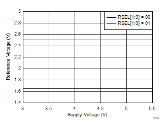
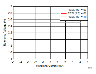
| VREFOUT | Reference output voltage at pin REFOUT | RSEL[1:0] = 00, no load | 2.45 | 2.5 | 2.55 | V | ||
| RSEL[1:0] = 01, no load | 1.6 | 1.65 | 1.7 | |||||
| RSEL[1:0] = 1x, no load | 45 | 50 | 55 | % of VDD | ||||
| Reference output voltage drift | RSEL[1:0] = 00, 01 | –50 | ±10 | 50 | ppm/°C | |||
| Voltage divider gain error drift | RSEL[1:0] = 1x | –50 | ±10 | 50 | ppm/°C | |||
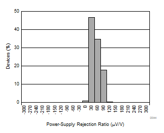
| PSRRREF | Power-supply rejection ratio | RSEL[1:0] = 00, 01 | –300 | ±15 | 300 | µV/V | ||
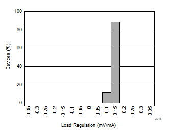
| Load regulation | RSEL[1:0] = 0x, load to GND or VDD, ΔILOAD = 0 mA to 5 mA, TA = –40°C to +125°C |
0.15 | 0.35 | mV/mA | ||||
| RSEL[1:0] = 1x, load to GND or VDD, ΔILOAD = 0 mA to 5 mA, TA = –40°C to +125°C |
0.3 | 0.8 | ||||||
| ISC | Short-circuit current | REFOUT connected to VDD | 20 | mA | ||||
| REFOUT connected to GND | –18 | |||||||
| DIGITAL INPUTS/OUTPUTS | ||||||||
| Logic Inputs (CMOS) | ||||||||
| VIH | High-level input voltage | TA = –40°C to +125°C | 0.7 × VDD | VDD + 0.3 | V | |||
| VIL | Low-level input voltage | TA = –40°C to +125°C | –0.3 | 0.3 × VDD | V | |||
| Input leakage current | 0.01 | µA | ||||||
| Logic Outputs (Open-Drain) | ||||||||
| VOH | High-level output voltage | Set by external pull-up resistor | V | |||||
| VOL | Low-level output voltage | 4-mA sink | 0.3 | V | ||||
| POWER SUPPLY | ||||||||
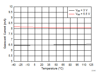
| IQ | Quiescent current | IICOMP1 = IICOMP2 = 0 mA, 3.0 V ≤ VDD ≤ 3.6 V, TA = –40°C to +125°C | 6.5 | 9 | mA | |||
| IICOMP1 = IICOMP2 = 0 mA, 4.5 V ≤ VDD ≤ 5.5 V, TA = –40°C to +125°C | 8.1 | 11 | ||||||
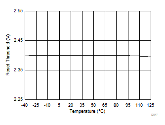
| VRST | Power-on reset threshold | 2.4 | V | |||||
(1) Fluxgate sensor front-end offset can be reduced using the Magnetic Core Demagnetization feature.
(2) Parameter value referred to output (RTO).
6.6 Typical Characteristics
at VDD = 5 V and TA = +25°C (unless otherwise noted)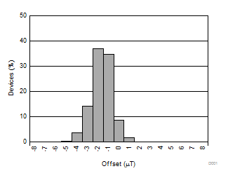
| VDD = 5 V |
Supply Voltage
Histogram
Negative Peak Current
| RLOAD = 20 Ω |
| VDD = 5 V |
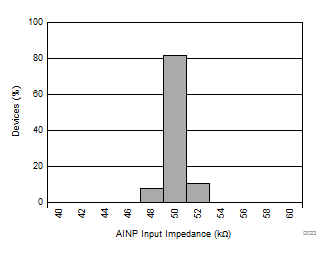
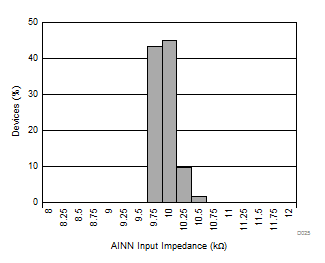
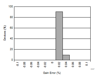
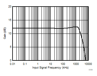
Frequency
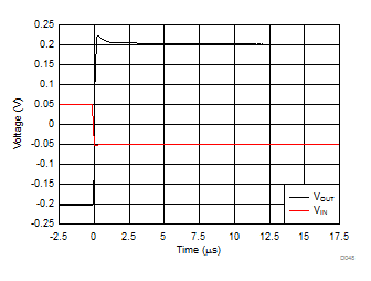
| Falling Edge |
Settling Time
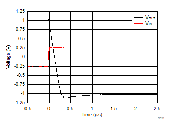
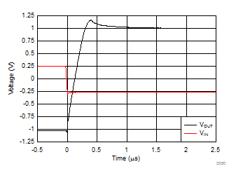
| Falling Edge |
Settling Time
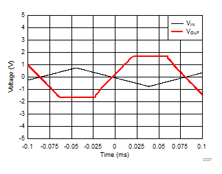
| VDD = 3.3 V |
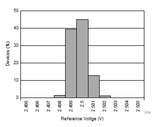
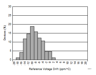
| VDD = 3.3 V |
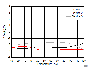
Temperature
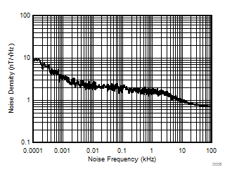
Noise Frequency
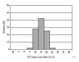
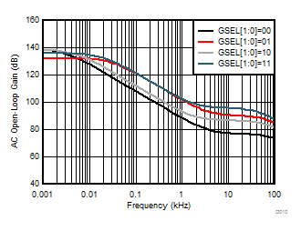
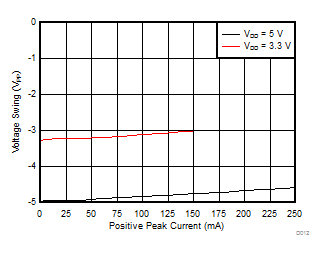
Positive Peak Current
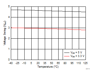
| RLOAD = 20 Ω |
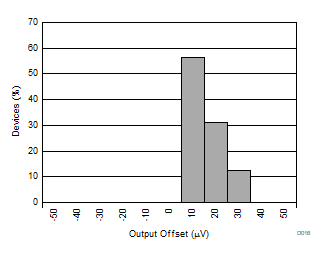
| VDD = 3.3 V |
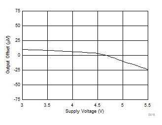
Supply Voltage
| Rising Edge |
Settling Time
| Rising Edge |
Settling Time
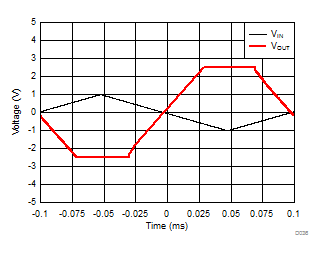
| VDD = 5 V |
