SBOS729A October 2015 – March 2016 DRV425
PRODUCTION DATA.
- 1 Features
- 2 Applications
- 3 Description
- 4 Revision History
- 5 Pin Configuration and Functions
- 6 Specifications
- 7 Detailed Description
- 8 Application and Implementation
- 9 Power-Supply Recommendations
- 10Layout
- 11Device and Documentation Support
- 12Mechanical, Packaging, and Orderable Information
Package Options
Mechanical Data (Package|Pins)
- RTJ|20
Thermal pad, mechanical data (Package|Pins)
- RTJ|20
Orderable Information
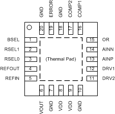
5 Pin Configuration and Functions
RTJ Package
20-Pin WQFN
Top View

Pin Functions
| PIN | I/O | DESCRIPTION | |
|---|---|---|---|
| NAME | NO. | ||
| AINN | 14 | I | Inverting input of the shunt-sense amplifier |
| AINP | 13 | I | Noninverting input of the shunt-sense amplifier |
| BSEL | 1 | I | Filter bandwidth select input |
| COMP1 | 16 | I | Internal compensation coil input 1 |
| COMP2 | 17 | I | Internal compensation coil input 2 |
| DRV1 | 12 | O | Compensation coil driver output 1 |
| DRV2 | 11 | O | Compensation coil driver output 2 |
| ERROR | 19 | O | Error flag: open-drain, active-low output |
| GND | 7, 10, 18, 20 | — | Ground reference |
| OR | 15 | O | Shunt-sense amplifier overrange indicator: open-drain, active-low output |
| PowerPAD | — | Connect the thermal pad to GND | |
| REFIN | 5 | I | Common-mode reference input for the shunt-sense amplifier |
| REFOUT | 4 | O | Voltage reference output |
| RSEL0 | 3 | I | Voltage reference mode selection input 0 |
| RSEL1 | 2 | I | Voltage reference mode selection input 1 |
| VDD | 8, 9 | — | Supply voltage, 3.0 V to 5.5 V. Decouple both pins using 1-µF ceramic capacitors placed as close as possible to the device. See the Power-Supply Decoupling and Layout sections for further details. |
| VOUT | 6 | O | Shunt-sense amplifier output |