SLVSCK2A April 2014 – February 2016 DRV8307
PRODUCTION DATA.
- 1 Features
- 2 Applications
- 3 Description
- 4 Revision History
- 5 Pin Configurations and Functions
- 6 Specifications
-
7 Detailed Description
- 7.1 Overview
- 7.2 Functional Block Diagram
- 7.3 Feature Description
- 7.4 Device Functional Modes
- 8 Application and Implementation
- 9 Power Supply Recommendations
- 10Layout
- 11Device and Documentation Support
- 12Mechanical, Packaging, and Orderable Information
Package Options
Mechanical Data (Package|Pins)
- RHA|40
Thermal pad, mechanical data (Package|Pins)
- RHA|40
Orderable Information
7 Detailed Description
7.1 Overview
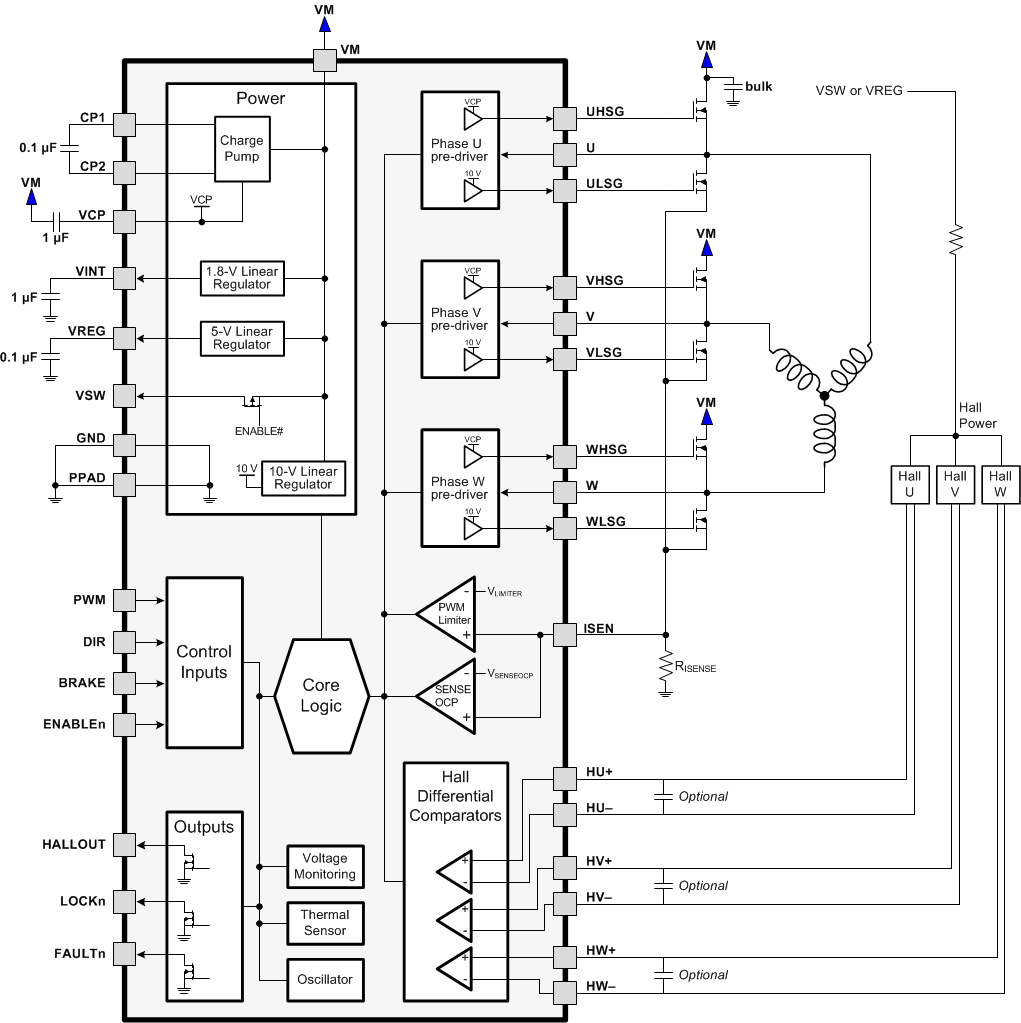
The DRV8307 device controls 3-phase brushless DC motors using a speed and direction input interface and Hall signals from the motor. The device drives N-channel MOSFETs with 10-V VGS and a gate drive current of 30 mA.
The speed of the motor is controlled by varying the duty cycle of the input clock (pulse-width modulation). Motor speed is indicated on the HALLOUT terminal, which follows the HALL U transitions.
When the DRV8307 device begins spinning a motor, it initially uses all three Hall sensor phases to commutate. After a constant speed is reached, the LOCKn terminal is pulled low and only one Hall sensor becomes used; this feature reduces jitter by eliminating the error caused by non-ideal Hall device placement and matching.
Numerous protection circuits prevent system components from being damaged during adverse conditions. Monitored aspects include motor voltage and current, gate drive voltage and current, device temperature, and rotor lockup. When a fault occurs, the DRV8307 device stops driving and pulls FAULTn low, in order to prevent FET damage and motor overheating.
The DRV8307 device is packaged in a compact 6 × 6-mm, 40-terminal VQFN with a 0.5-mm terminal pitch, and operates through an industrial ambient temperature range of –40°C to 85°C.
7.2 Functional Block Diagram
7.3 Feature Description
7.3.1 Hall Comparators
Three comparators are provided to process the raw signals from Hall effect transducers to commutate the motor. The Hall amplifiers sense zero crossings of the differential inputs and pass the information to digital logic.
The Hall amplifiers have hysteresis, and their detect threshold is centered at 0. Note, hysteresis is defined as shown in Figure 3:
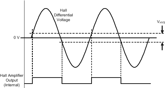 Figure 3. Hall Amplifier Hysteresis
In addition to hysteresis, the Hall inputs are deglitched with a circuit that ignores any extra Hall transitions for a period of 20 μs after sensing a valid transition. This prevents PWM noise from being coupled into the Hall inputs, which can result in erroneous commutation.
If excessive noise is still coupled into the Hall comparator inputs, it may be necessary to add capacitors between the + and – inputs of the Hall comparators, and (or) between the input or inputs and ground.
The ESD protection circuitry on the Hall inputs implements a diode to VREG. Because of this diode, the voltage on the Hall inputs should not exceed the VREG voltage.
Since VREG is disabled in standby mode (ENABLEn inactive), the Hall inputs should not be driven by external voltages in standby mode. The DRV8307 device specifies if the Hall sensors are powered from VREG or VSW; however, if the Hall sensors are powered externally, they should be disabled when the DRV8307 is put into standby mode. In addition, the Hall sensors should be powered-up before enabling the motor, or an invalid Hall state may cause a delay in motor operation.
7.3.2 HALLOUT Output
The HALLOUT terminal indicates the speed of the motor. It follows the transitions observed from the HALL U hall sensor. Figure 4 shows the HALLOUT signal.
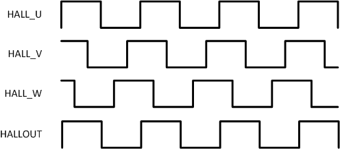 Figure 4. HALLOUT Relationship to Hall Transitions
7.3.3 Enable, Reset, and Clock Generation
The ENABLEn terminal is used to start and stop motor operation. The ENABLEn terminal is active low.
When ENABLEn is active, operation of the motor is enabled. When ENABLEn is made inactive, the motor coasts. After motor rotation has stopped (when no transitions occur on the HALLOUT terminal for a period of 1 s), the DRV8307 device enters a low-power standby state.
When in the standby state:
- The motor driver circuitry is disabled (all gate drive outputs are driven low, so the FET outputs are high-impedance).
- The gate drive regulator and charge pump are disabled.
- The VREG regulator and VSW power switch are disabled.
- All analog circuitry is placed into a low power state.
- The digital circuitry in the device still operates.
All internal logic is reset in two different ways:
- Upon device power-up
- When VM drops below VRESET
An internal clock generator provides all timing for the DRV8307 device. The master oscillator runs at 100 MHz. This clock is divided to a nominal 50-MHz frequency that clocks the remainder of the digital logic.
7.3.4 Commutation
For 3-phase brushless DC motors, rotor position feedback is provided from Hall effect transducers mounted on the motor. These transducers provide three overlapping signals, each 60° apart. The windings are energized in accordance with the signals from the Hall sensors to cause the motor to move.
In addition to the Hall sensor inputs, commutation is affected by a direction control, which alters the direction of motion by reversing the commutation sequence. Control of commutation direction is by the DIR input terminal.
If the commanded direction changes while the motor is moving, the device allows the motor to coast until the motor stops. The stopped condition is determined by measuring the period of the HALL_U signal; when the period exceeds 160 ms, typical operation resumes and the motor starts spinning in the commanded direction. This prevents excessive current flow in the output stage if the motor is reversed while running at speed.
In standard 120° commutation, mis-positioning the Hall sensors can cause motor noise, vibration, and torque ripple. 120° commutation using a single Hall sensor (single-Hall commutation) can improve motor torque ripple and vibration because it relies on only one Hall edge for timing.
7.3.4.1 120° 3-Hall Commutation
In standard 120° commutation, the motor phases are energized using simple combination logic based on all three Hall sensor inputs.
Standard 120° commutation is in accordance with Table 1, Figure 5, and Figure 6:
Table 1. Standard 120° Commutation(1)
| STATE | HALL INPUTS | PRE-DRIVE OUTPUTS | ||||||||||
|---|---|---|---|---|---|---|---|---|---|---|---|---|
| DIR = 1 | DIR = 0 | Phase U | Phase V | Phase W | ||||||||
| U_H | V_H | W_H | U_H | V_H | W_H | U_HSGATE | U_LSGATE | V_HSGATE | V_LSGATE | W_HSGATE | W_LSGATE | |
| 1 | L | L | H | H | H | L | L | L | PWM | L / !PWM(2) | L | H |
| 2 | L | H | H | H | L | L | PWM | L / !PWM(2) | L | L | L | H |
| 3 | L | H | L | H | L | H | PWM | L / !PWM(2) | L | H | L | L |
| 4 | H | H | L | L | L | H | L | L | L | H | PWM | L / !PWM(2) |
| 5 | H | L | L | L | H | H | L | H | L | L | PWM | L / !PWM(2) |
| 6 | H | L | H | L | H | L | L | H | PWM | L / !PWM(2) | L | L |
| 1X | H | H | H | L | L | L | L | L | L | L | L | L |
| 2X | L | L | L | H | H | H | L | L | L | L | L | L |
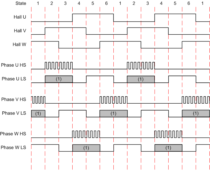
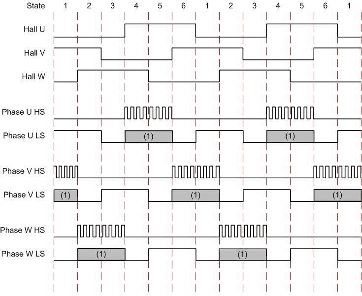 Figure 6. Standard 120° Commutation (DIR = 0)
7.3.4.2 120° Single-Hall Commutation
To generate commutation timing for single-Hall commutation, a digital timer is used to create a clock that runs at 960× the Hall sensor frequency. Only one Hall sensor input, HALL_U, is used for commutation; this eliminates any torque ripple caused by mechanical or electrical offsets of individual Hall sensors.
Single-Hall commutation is only enabled when the motor is operating at a nearly constant speed or speed-locked condition. To control this function, logic is used to determine when the speed is constant. This logic generates the LOCK signal. The LOCK signal is also output on the LOCKn terminal.
Until LOCK goes active (for example, at start-up, stop, or application of a sudden load that causes motor speed to drop very quickly), standard 120° commutation is used requiring all three Hall sensors.
Timing of 120° single-Hall commutation is essentially the same as standard 120° commutation shown previously. However, there are small time differences in when the transitions occur.
7.3.5 Braking
Motor braking can be initiated by the BRAKE terminal.
Table 2. Brake Behavior
| BRAKE Terminal | Resulting Function |
|---|---|
| 0 | Not brake |
| 1 | Brake |
When the motor is braking, all low-side drivers are held in an on state, causing all low-side FETs to turn on.
7.3.6 Output Pre-Drivers
The output drivers for each phase consist of N-channel and P-channel MOSFET devices arranged as a CMOS buffer. They are designed to directly drive the gate of external N-channel power MOSFETs. The outputs provide synchronous rectification operation. In synchronous rectification, the low-side FET is turned on when the high side is turned off.
The high-side gate drive output UHSG is driven to VCP whenever the duty cycle output U_PD from the PWM generator is high, the enable signal U_HS from the commutation logic is active, and the current limit (VLIMITER) is not active. If the high-side FET is on and a current limit event occurs, the high-side FET is immediately turned off until the next PWM cycle.
The low-side gate drive ULSG is driven to VOUTL whenever the internal signal U_LS is high, or whenever synchronous rectification is active and UHSG is low.
Phases V and W operate in an identical fashion.
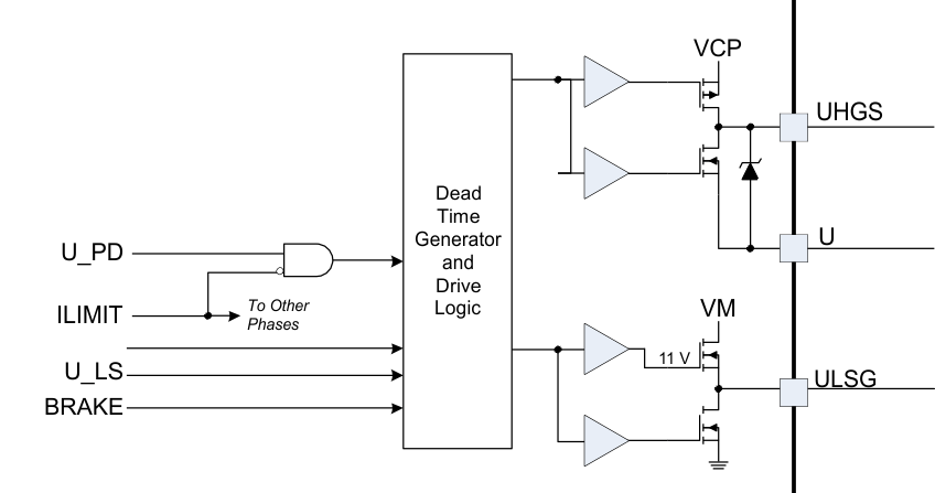 Figure 7. Pre-Driver Block Diagram
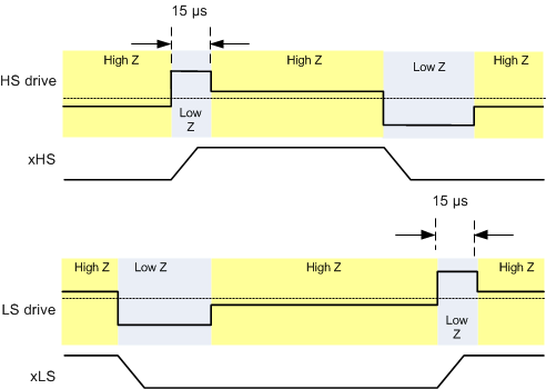 Figure 8. Gate Control Behavior
The peak drive current of the pre-drivers is fixed at 30 mA.
When changing the state of the output, the peak current is applied for a short period of time (15 μs) to charge the gate capacitance. After this time, a weak current source is used to keep the gate at the desired state.
During high-side turn-on, the low-side gate is held low with a low impedance. This prevents the gate-source capacitance of the low-side FET from inducing turn-on. Similarly, during low-side turn-on, the high-side gate is held off with a low impedance.
The pre-driver circuits include enforcement of a dead time in analog circuitry, which prevents the high-side and low-side FETs from conducting at the same time.
7.3.7 Current Limit
The current limit circuit activates if the voltage detected across the low-side sense resistor exceeds VLIMITER. Note that the current limit circuit is ignored immediately after the PWM signal goes active for a short blanking time, to prevent false trips of the current limit circuit.
If current limit activates, the high-side FET is disabled until the beginning of the next PWM cycle. If synchronous rectification is enabled when the current limit activates, the low-side FET is activated while the high-side FET is disabled.
7.3.8 Charge Pump
Since the output stages use N-channel FETs, a gate drive voltage higher than the VM power supply is needed to fully enhance the high-side FETs. The DRV8307 device integrates a charge pump circuit that generates a voltage approximately 10 V more than the VM supply for this purpose.
The charge pump requires two external capacitors for operation. For details on these capacitors (value, connection, and so forth), refer to Figure 9.
The charge pump is shut down when in standby mode (ENABLEn inactive).
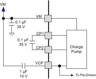 Figure 9. Charge Pump Block Diagram
7.3.9 5-V Linear Regulator
A 5-V linear regulator (VREG) is provided to power internal logic and external circuitry, such as the Hall effect sensors.
A capacitor must be connected from the VREG output to ground, even if the output is not used for external circuitry. The recommended capacitor value is a 0.1-μF, 10-V ceramic capacitor.
The VREG output is designed to provide up to 30-mA output current, but power dissipation and thermal conditions must be considered. As an example, with 24 V in and 20 mA out, power dissipated in the linear regulator is 19 V × 20 mA = 380 mW.
The VREG regulator is shutdown in standby mode (when ENABLEn is inactive).
7.3.10 Power Switch
A low-current switch is provided in the DRV8307 device that can be used to power the Hall sensors or other external circuitry through the VSW terminal. When ENABLEn is active the switch is turned on, connecting the VSW terminal to VM. When ENABLEn is inactive the switch is turned off (standby mode).
7.3.11 Protection Circuits
A number of protection circuits are included in the DRV8307 device. Faults are reported by asserting the FAULTn terminal (an active-low, open-drain output signal).
7.3.11.1 VM Undervoltage Lockout (UVLO)
If the VM power supply drops, there may not be enough voltage to fully turn on the output FETs. Operation in this condition causes excessive heating in the output FETs. To protect against this, the DRV8307 device contains an UVLO circuit.
In the event that the VM supply voltage drops below the UVLO threshold (VUVLO), the FAULTn terminal is driven active and the motor driver is disabled. After VM returns to a voltage above the UVLO threshold, the FAULTn terminal is high impedance and operation of the motor driver automatically resumes.
7.3.11.2 VM Overvoltage (VMOV)
In some cases, energy from the mechanical system can be forced back into the VM power supply. This can result in the VM power supply being boosted by the energy in the mechanical system, causing breakdown of the output FETs, or damaging the DRV8307 device. To protect against this, the DRV8307 device has overvoltage protection.
An overvoltage event is recognized if the VM voltage exceeds the overvoltage threshold (VMOVLO). Note that for the output FETs to be protected, they must be rated for a voltage greater than the selected overvoltage threshold.
In the event of an overvoltage, the FAULTn terminal is pulled low. The output stage is forced into asynchronous rectification. After VM returns to a voltage below the overvoltage threshold, the FAULTn terminal is high impedance. After a fixed 60-μs delay, synchronous rectification is re-enabled.
7.3.11.3 Motor Overcurrent Protection (OCP)
OCP is provided on each FET in addition to the current limit circuit. The OCP circuit is designed to protect the output FETs from atypical conditions such as a short circuit between the motor outputs and each other, power, or ground.
The OCP circuit is independent from the current limit circuitry. OCP works by monitoring the voltage drop across the external FETs when they are enabled. If the voltage across a driven FET exceeds VFETOCP for more than tFETOCP an OCP event is recognized.
In addition to monitoring the voltage across the FETs, an OCP event is triggered if the voltage applied to the ISEN terminal exceeds the VSENSEOCP threshold voltage.
In the event of an OCP event, FAULTn is pulled low and the motor driver is disabled.
After a fixed delay of 5 ms, the FAULTn terminal is driven inactive and the motor driver is re-enabled.
7.3.11.4 Charge Pump Failure (CPFAIL)
If the voltage generated by the high-side charge pump is too low, the high-side output FETs are not fully turned on and excessive heating results. To protect against this, the DRV8307 device has a circuit that monitors the charge pump voltage.
If the charge pump voltage drops below VCPFAIL, the FAULTn terminal is pulled low and the motor driver is disabled. After the charge pump voltage returns to a voltage above the VCPFAIL threshold, the FAULTn terminal is high impedance and operation of the motor driver automatically resumes.
7.3.11.5 Charge Pump Short (CPSC)
To protect against excessive power dissipation inside the DRV8307 device, a circuit monitors the charge pump and disables it in the event of a short circuit on the PCB.
If a short circuit is detected on the charge pump, the FAULTn terminal is pulled low and the motor driver is disabled. After a fixed period of 5 s, the FAULTn terminal is high impedance and operation of the motor driver automatically resumes. If the short circuit condition is still present, the cycle repeats.
7.3.11.6 Rotor Lockup (RLOCK)
Circuitry in the DRV8307 device detects a locked or stalled rotor. This RLOCK can occur in the event of a mechanical jam or excessive torque load that causes the motor to stop rotating while enabled. The rotor lock condition is set if there are no transitions detected on the HALLOUT signal for 3 s. RLOCK can also occur if the three Hall signals are an invalid state (all High or all Low), which can be caused by a bad wire connection. If the BRAKE terminal goes high for longer than 3 s while the PWM clock is on DRV8307 will detect RLOCK.
If a locked rotor condition is recognized, the FAULTn terminal is pulled low and the motor driver is disabled. The part re-enables itself after a fixed delay of 5 s.
7.3.11.7 Overtemperature (OTS)
To protect against any number of faults that could result in excessive power dissipation inside the device, the DRV8307 device includes overtemperature protection.
Overtemperature protection activates if the temperature of the die exceeds the OTS threshold temperature (TTSD). If this occurs, the FAULTn terminal is pulled low and the device is disabled. The part re-enables itself after a fixed delay of 5 s.
7.4 Device Functional Modes
7.4.1 Clock PWM Mode
In PWM input mode, the PWM input signal is timed using a 50-MHz clock to generate a 12-bit number that corresponds to the duty cycle of the incoming PWM signal. The input PWM frequency should be between 16 and 50 kHz; higher PWM frequencies work, but resolution is degraded. Note that the gate driver’s output PWM frequency is independent of the speed control PWM input frequency; the output PWM frequency is 25 kHz.
The outputs of the PWM generators are the signals U_PD, V_PD, and W_PD. These contain the duty cycle information for each phase.
Figure 10 shows modulation and PWM generation.
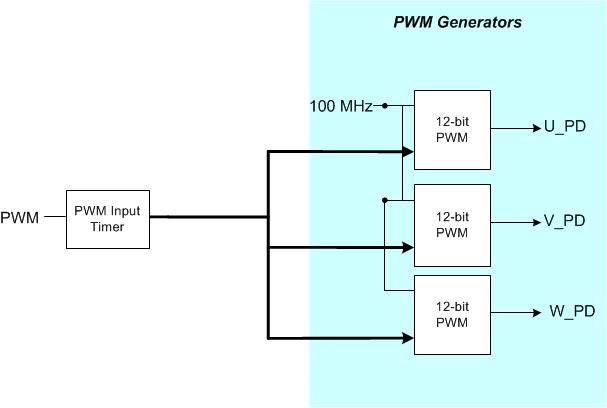 Figure 10. Modulation and PWM Generation
When the DRV8307 is driving a motor, the motor should not be stopped by setting the PWM input to 0% duty cycle. Instead, ENABLEn should be brought high.