SLES242G December   2009  – December 2014 DRV8412

PRODUCTION DATA.  

  1. Features
  2. Applications
  3. Description
    1.     Simplified Application Diagram
  4. Revision History
  5. Pin Configuration and Functions
    1.     Pin Functions
  6. Specifications
    1. 6.1 Absolute Maximum Ratings
    2. 6.2 ESD Ratings
    3. 6.3 Recommended Operating Conditions
    4. 6.4 Thermal Information
    5. 6.5 Package Heat Dissipation Ratings
    6. 6.6 Package Power Deratings (DRV8412)
    7. 6.7 Electrical Characteristics
    8. 6.8 Typical Characteristics
  7. Detailed Description
    1. 7.1 Overview
    2. 7.2 Functional Block Diagram
    3. 7.3 Feature Description
      1. 7.3.1 Error Reporting
      2. 7.3.2 Device Protection System
        1. 7.3.2.1 Bootstrap Capacitor Undervoltage Protection
        2. 7.3.2.2 Overcurrent (OC) Protection
        3. 7.3.2.3 Overtemperature Protection
        4. 7.3.2.4 Undervoltage Protection (UVP) and Power-On Reset (POR)
      3. 7.3.3 Device Reset
    4. 7.4 Device Functional Modes
  8. Application and Implementation
    1. 8.1 Application Information
    2. 8.2 Typical Applications
      1. 8.2.1 Full Bridge Mode Operation
        1. 8.2.1.1 Design Requirements
        2. 8.2.1.2 Detailed Design Procedure
          1. 8.2.1.2.1 Motor Voltage
          2. 8.2.1.2.2 Current Requirement of 12-V Power Supply
          3. 8.2.1.2.3 Voltage of Decoupling Capacitor
          4. 8.2.1.2.4 Overcurrent Threshold
          5. 8.2.1.2.5 Sense Resistor
        3. 8.2.1.3 Application Curves
      2. 8.2.2 Parallel Full Bridge Mode Operation
      3. 8.2.3 Stepper Motor Operation
      4. 8.2.4 TEC Driver
      5. 8.2.5 LED Lighting Driver
  9. Power Supply Recommendations
    1. 9.1 Bulk Capacitance
    2. 9.2 Power Supplies
    3. 9.3 System Power-Up and Power-Down Sequence
      1. 9.3.1 Powering Up
      2. 9.3.2 Powering Down
    4. 9.4 System Design Recommendations
      1. 9.4.1 VREG Pin
      2. 9.4.2 VDD Pin
      3. 9.4.3 OTW Pin
      4. 9.4.4 Mode Select Pin
      5. 9.4.5 Parallel Mode Operation
      6. 9.4.6 TEC Driver Application
  10. 10Layout
    1. 10.1 Layout Guidelines
      1. 10.1.1 PCB Material Recommendation
      2. 10.1.2 Ground Plane
      3. 10.1.3 Decoupling Capacitor
      4. 10.1.4 AGND
    2. 10.2 Layout Example
      1. 10.2.1 Current Shunt Resistor
    3. 10.3 Thermal Considerations
      1. 10.3.1 DRV8412 Thermal Via Design Recommendation
  11. 11Device and Documentation Support
    1. 11.1 Related Links
    2. 11.2 Trademarks
    3. 11.3 Electrostatic Discharge Caution
    4. 11.4 Glossary
  12. 12Mechanical, Packaging, and Orderable Information

Package Options

Mechanical Data (Package|Pins)
Thermal pad, mechanical data (Package|Pins)
Orderable Information

DRV8412 Thermal Via Design Recommendation

Thermal pad of the DRV8412 is attached at bottom of device to improve the thermal capability of the device. The thermal pad has to be soldered with a very good coverage on PCB in order to deliver the power specified in the datasheet. The figure below shows the recommended thermal via and land pattern design for the DRV8412. For additional information, see TI application report, PowerPad Made Easy (SLMA004) and PowerPad Layout Guidelines (SOLA120).
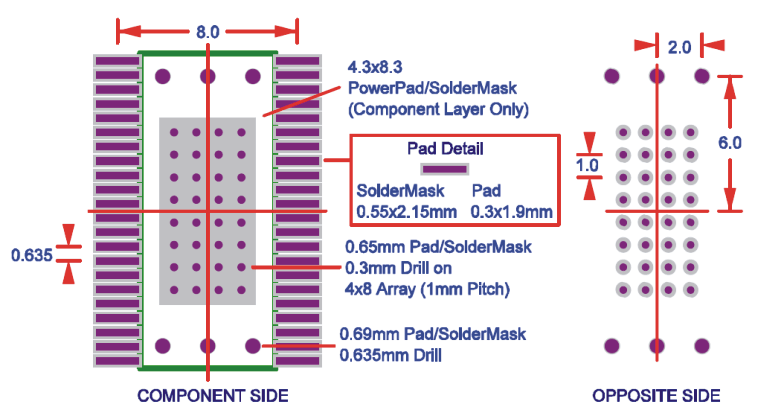
DRV8412 DRV8432 thermal_vias_242.gifFigure 23. DRV8412 Thermal Via Footprint