SLVSC40H June 2013 – May 2020 DRV8711
PRODUCTION DATA.
- 1 Features
- 2 Applications
- 3 Description
- 4 Revision History
- 5 Pin Configuration and Functions
- 6 Specifications
-
7 Detailed Description
- 7.1 Overview
- 7.2 Functional Block Diagram
- 7.3 Feature Description
- 7.4 Device Functional Modes
- 7.5 Programming
- 7.6
Register Maps
- 7.6.1 Control Registers
- 7.6.2 CTRL Register (Address = 0x00)
- 7.6.3 TORQUE Register (Address = 0x01)
- 7.6.4 OFF Register (Address = 0x02)
- 7.6.5 BLANK Register (Address = 0x03)
- 7.6.6 DECAY Register (Address = 0x04)
- 7.6.7 STALL Register (Address = 0x05)
- 7.6.8 DRIVE Register (Address = 0x06)
- 7.6.9 STATUS Register (Address = 0x07)
- 8 Application and Implementation
- 9 Power Supply Recommendations
- 10Layout
- 11Device and Documentation Support
- 12Mechanical, Packaging, and Orderable Information
Package Options
Mechanical Data (Package|Pins)
- DCP|38
Thermal pad, mechanical data (Package|Pins)
- DCP|38
Orderable Information
7.3.2 Direct PWM Input Mode
Direct PWM mode is selected by setting the PWMMODE bit in the OFF register. In direct PWM input mode, the AIN1, AIN2, BIN1, and BIN2 directly control the state of the output drivers. This allows for driving up to two brushed DC motors. The logic is shown in Table 2:
Table 2. Direct PWM Input Mode Logic
| xIN1 | xIN2 | xOUT1 | xOUT2 | OPERATION |
|---|---|---|---|---|
| 0 | 0 | Z | Z | Asynchronous Fast Decay |
| 0 | 1 | L | H | Reverse Drive |
| 1 | 0 | H | L | Forward Drive |
| 1 | 1 | L | L | Slow Decay |
If mixed or auto-mixed decay modes are used, they will apply to every cycle, because current change information is not available.
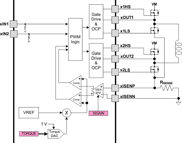
In direct PWM mode, the current control circuitry is still active. The full-scale VREF is set to 2.75 V. The TORQUE register may be used to scale this value, and the ISEN sense amp gain may still be set using the ISGAIN bits of the CTRL register.
 Figure 7. Direct PWM Input Mode
 The current through the motor windings is regulated by an adjustable fixed-off-time PWM current regulation circuit. When an H-bridge is enabled, current rises through the winding at a rate dependent on the DC voltage and inductance of the winding and the magnitude of the back EMF present. Once the current hits the current chopping threshold, the bridge disables the current for a fixed period of time, which is programmable between 500 ns and 128 µs by writing to the TOFF bits in the OFF register. After the off time expires, the bridge is re-enabled, starting another PWM cycle.
The chopping current is set by a comparator which compares the voltage across a current sense resistor connected to the xISENx pins, multiplied by the gain of the current sense amplifier, with a reference voltage. The current sense amplifier is programmable in the CTRL register. When driving in PWM mode, the chopping current is calculated as follows:

Where TORQUE is the setting of the TORQUE bits, and ISGAIN is the programmed gain of the ISENSE amplifiers (5, 10, 20, or 40).