SLVSC40H June 2013 – May 2020 DRV8711
PRODUCTION DATA.
- 1 Features
- 2 Applications
- 3 Description
- 4 Revision History
- 5 Pin Configuration and Functions
- 6 Specifications
-
7 Detailed Description
- 7.1 Overview
- 7.2 Functional Block Diagram
- 7.3 Feature Description
- 7.4 Device Functional Modes
- 7.5 Programming
- 7.6
Register Maps
- 7.6.1 Control Registers
- 7.6.2 CTRL Register (Address = 0x00)
- 7.6.3 TORQUE Register (Address = 0x01)
- 7.6.4 OFF Register (Address = 0x02)
- 7.6.5 BLANK Register (Address = 0x03)
- 7.6.6 DECAY Register (Address = 0x04)
- 7.6.7 STALL Register (Address = 0x05)
- 7.6.8 DRIVE Register (Address = 0x06)
- 7.6.9 STATUS Register (Address = 0x07)
- 8 Application and Implementation
- 9 Power Supply Recommendations
- 10Layout
- 11Device and Documentation Support
- 12Mechanical, Packaging, and Orderable Information
Package Options
Mechanical Data (Package|Pins)
- DCP|38
Thermal pad, mechanical data (Package|Pins)
- DCP|38
Orderable Information
7.3.7 Predrivers
An internal charge pump circuit and predrivers inside the DRV8711 directly drive N-channel MOSFETs, which drive the motor current.
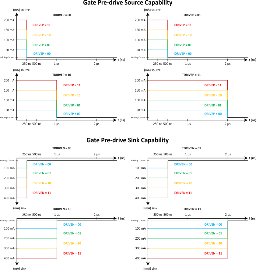
The peak drive current of the predrivers is adjustable by setting the bits in the DRIVE register. Peak source currents may be set to 50 mA, 100 mA, 150 mA, or 200 mA. The peak sink current is approximately 2x the peak source current. Adjusting the peak current will change the output slew rate, which also depends on the FET input capacitance and gate charge.
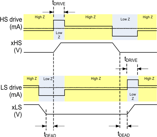
When changing the state of the output, the peak current is applied for a short period of time (tDRIVE), to charge the gate capacitance. After this time, a weak current source is used to keep the gate at the desired state. When selecting the gate drive strength for a given external FET, the selected current must be high enough to fully charge and discharge the gate during the time when driven at full current, or excessive power will be dissipated in the FET.
During high-side turnon, the low-side gate is pulled low. This prevents the gate-source capacitance of the low-side FET from inducing turnon.
The predriver circuits include enforcement of a dead time in analog circuitry, which prevents the high-side and low-side FETs from conducting at the same time. Additional dead time is added with digital delays. This delay can be selected by setting the DTIME bits in the CTRL register.
 Figure 13. Predrivers
  Figure 14. Gate Pre-Drive Source/Sink Capability