SLVSBA3C June 2012 – December 2015 DRV8806
PRODUCTION DATA.
- 1 Features
- 2 Applications
- 3 Description
- 4 Revision History
- 5 Pin Configuration and Functions
- 6 Specifications
- 7 Detailed Description
- 8 Application and Implementation
- 9 Power Supply Recommendations
- 10Layout
- 11Device and Documentation Support
- 12Mechanical, Packaging, and Orderable Information
Package Options
Mechanical Data (Package|Pins)
- PWP|16
Thermal pad, mechanical data (Package|Pins)
- PWP|16
Orderable Information
7 Detailed Description
7.1 Overview
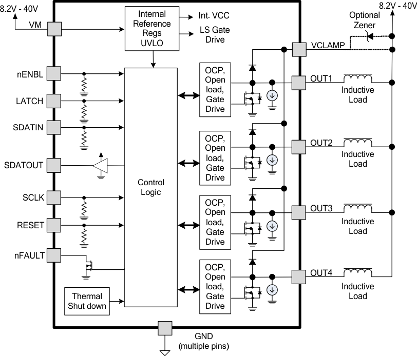
The DRV8806 is an integrated 4-channel low-side driver controlled using a serial interface to change the state of the low-side driver outputs. The low-side driver outputs consist of four N-channel MOSFETs that have a typical RDS(ON) of 500 mΩ. A single motor supply input VM serves as device power and is internally regulated to power the low-side gate drive. Data is shifted into a temporary data register in the device through the SDATIN pin, one bit at each rising edge of SCLK, while LATCH is held low. The outputs of the device can be disabled by pulling nENBL logic high. Several safety features are integrated in the device including overcurrent protection, thermal shutdown, undervoltage lockout, and open load protection. The overcurrent protection and open load faults share a fault bit per channel that is set when one of these conditions occurs.
7.3 Feature Description
7.3.1 Output Drivers
The DRV8806 contains four protected low-side drivers. Each output has an integrated clamp diode connected to a common pin, VCLAMP.
VCLAMP can be connected to the main power supply voltage, VM. It can also be connected to a Zener or TVS diode to VM, allowing the switch voltage to exceed the main supply voltage VM. This connection can be beneficial when driving loads that require very fast current decay, such as unipolar stepper motors.
In all cases, the voltage on the outputs must not be allowed to exceed the maximum output voltage specification.
7.3.2 Protection Circuits
The DRV8806 is fully protected against undervoltage, overcurrent and overtemperature events.
7.3.2.1 Overcurrent Protection (OCP)
An analog current limit circuit on each FET limits the current through the FET by removing the gate drive. If this analog current limit persists for longer than the tOCP deglitch time (approximately 3.5 µs), the driver will be disabled and the nFAULT pin will be driven low. The driver will remain disabled for the tRETRY retry time (approximately 1.2 ms), then the fault will be automatically cleared. The fault will be cleared immediately if either RESET pin is activated or VM is removed and reapplied.
7.3.2.2 Thermal Shutdown (TSD)
If the die temperature exceeds safe limits, all output FETs will be disabled and the nFAULT pin will be driven low. Once the die temperature has fallen to a safe level, operation will automatically resume.
7.3.2.3 Undervoltage Lockout (UVLO)
If at any time the voltage on the VM pin falls below the undervoltage lockout threshold voltage, all circuitry in the device will be disabled, and internal logic will be reset. Operation will resume when VM rises above the UVLO threshold.
7.4 Device Functional Modes
7.4.1 Serial Interface Operation
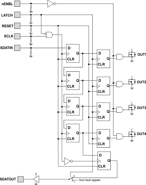
The DRV8806 is controlled with a simple serial interface. Logically, the interface is shown in Figure 6.
Data is shifted into a temporary holding shift register in the part using the SDATIN pin, one bit at each rising edge of the SCLK pin, while LATCH is low. Data is shifted from the last bit to the SDATOUT pin, so multiple devices may be daisy-chained together using a single serial interface.
Note that the SDATOUT pin has a push-pull driver, which can support driving another DRV8806 SDATIN pin at clock frequencies of up to 1 MHz without an external pullup. A pullup resistor can be used between SDATOUT and an external 5-V logic supply to support higher clock frequencies. TI recommends a resistor value of approximately 1 kΩ. The SDATOUT pin is capable of approximately 1-mA source and 5-mA sink. To supply logic signals to a lower-voltage microcontroller, use a resistor divider from SDATOUT to GND.
A rising edge on the LATCH pin latches the data from the temporary shift register into the output stage.
7.4.2 Fault Output Register
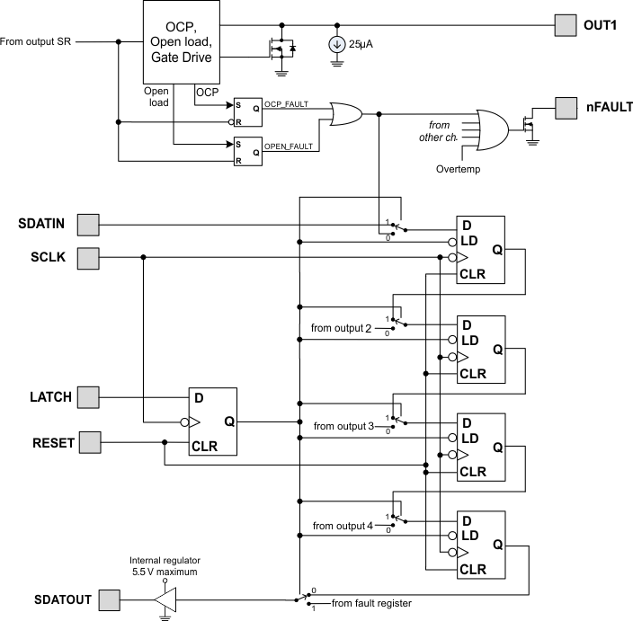
The DRV8806 contains circuitry to detect open or shorted loads. The status of the loads can be read through the serial interface. The logic is shown in Figure 7.
 Figure 7. Fault Output
To overcome any leakage currents to accurately sense an open load, a small current source is connected to each output pin. This source pulls approximately 25-µA of current to ground. The voltage on the output pin is sensed during the time that the output is off, and if the voltage on the pin is less than 1.2 V (indicating that there is no load connected) after the open load deglitch time, the OPEN_FAULT latch is set. This latch is cleared whenever the output bit is set.
When the output is turned on, if an overcurrent (OCP) fault is detected, the channel will be turned off and the OCP_FAULT latch is set. This latch will be cleared whenever the output bit is cleared.
The state of the OCP_FAULT and OPEN_FAULT signals is combined into a single fault bit per channel, and loaded into a shift register while the LATCH pin is low. When the LATCH pin is taken high, the fault data is latched into the shift register at the first falling edge of SCLK. Data may then be shifted out on the SDATOUT pin on each falling edge of the SCLK pin.
Note that the LATCH signal must be high for a minimum of 200 ns before valid data can be clocked out.
The nFAULT pin will be driven active low whenever any of the OCP_FAULT or OPEN_FAULT latches are set, as well as whenever there is an overtemperature condition.
7.4.3 Daisy-Chain Connection
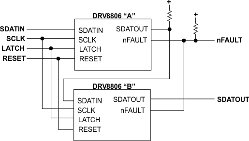
Two or more DRV8806 devices may be connected together to use a single serial interface. The SDATOUT pin of the first device in the chain is connected to the SDATIN pin of the next device. The SCLK, LATCH, RESET, and nFAULT pins are connected together.
 Figure 8. Daisy-Chain Connection
Figure 9 shows an example of a serial transaction, writing the output bits, and then reading the fault status bits, using two devices connected together in a daisy-chain.
Note that the LATCH signal must be high for a minimum of 200 ns before valid data can be clocked out.
 Figure 9. Daisy-Chain Serial Transaction
7.4.4 nENBL and RESET Operation
The nENBL pin enables or disables the output drivers. nENBL must be low to enable the outputs. nENBL does not affect the operation of the serial interface logic. Note that nENBL has an internal pulldown.
The RESET pin, when driven active high, resets internal logic, including the OCP fault. All serial interface registers are cleared. Note that RESET has an internal pulldown. An internal power-up reset is also provided, so it is not required to drive RESET at power up.

