SLVSAB9E May 2010 – November 2015 DRV8814
PRODUCTION DATA.
- 1 Features
- 2 Applications
- 3 Description
- 4 Revision History
- 5 Pin Configuration and Functions
- 6 Specifications
- 7 Detailed Description
- 8 Application and Implementation
- 9 Power Supply Recommendations
- 10Layout
- 11Device and Documentation Support
- 12Mechanical, Packaging, and Orderable Information
Package Options
Mechanical Data (Package|Pins)
- PWP|28
Thermal pad, mechanical data (Package|Pins)
- PWP|28
Orderable Information
8 Application and Implementation
NOTE
Information in the following applications sections is not part of the TI component specification, and TI does not warrant its accuracy or completeness. TI’s customers are responsible for determining suitability of components for their purposes. Customers should validate and test their design implementation to confirm system functionality.
8.1 Application Information
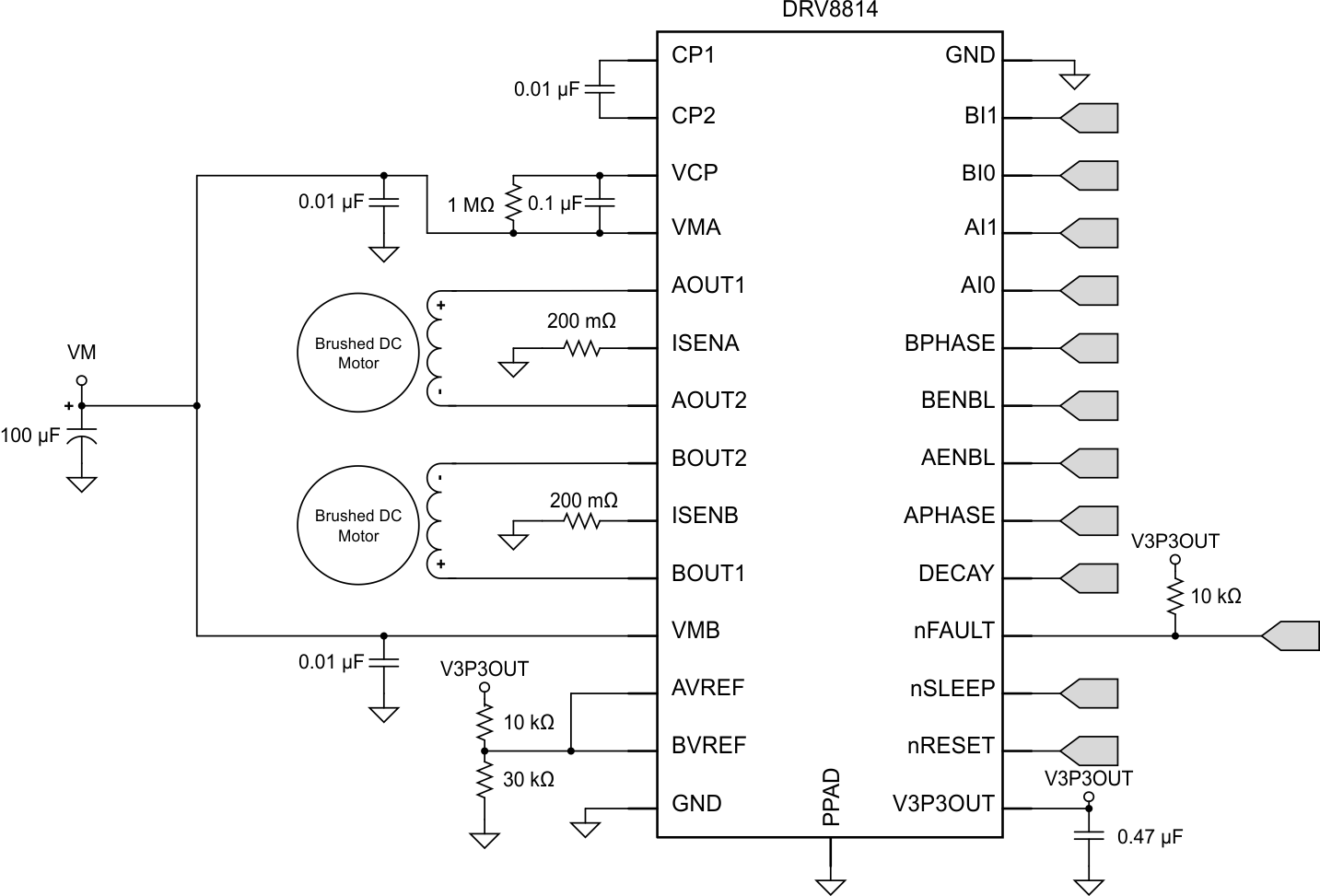
The DRV8814 can be used to control two brushed DC motors. The PHASE/ENBL interface controls the outputs and current control can be implemented with the internal current regulation circuitry. Detailed fault reporting is provided with the internal protection circuits and nFAULT pin.
8.2 Typical Application
 Figure 7. Typical Application Schematic
8.2.1 Design Requirements
Specific parameters for designing a dual brushed DC motor drive system.
Table 3. Design Parameters
| DESIGN PARAMETER | REFERENCE | EXAMPLE VALUE |
|---|---|---|
| Supply Voltage | VM | 24 V |
| Motor Winding Resistance | RL | 3.9 Ω |
| Moto Winding Inductance | IL | 2.9 mH |
| Sense Resistor Value | RSENSE | 200 mΩ |
| Target Full-Scale Current | IFS | 1.25 A |
8.2.2 Detailed Design Procedure
8.2.2.1 Current Regulation
In a stepper motor, the set full-scale current (IFS) is the maximum current driven through either winding. This quantity depends on the xVREF analog voltage and the sense resistor value (RSENSE). During stepping, IFS defines the current chopping threshold (ITRIP) for the maximum current step. The gain of DRV8814 is set for 5 V/V.

To achieve IFS = 1.25 A with RSENSE of 0.2 Ω, xVREF should be 1.25 V.
8.2.2.2 Decay Modes
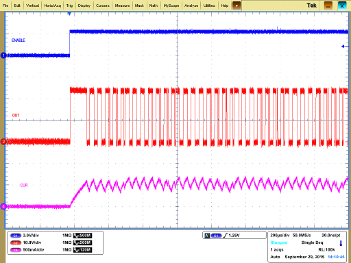
The DRV8814 supports two different decay modes: slow decay and fast decay. The current through the motor windings is regulated using a fixed-frequency PWM scheme. This means that after any drive phase, when a motor winding current has hit the current chopping threshold (ITRIP), the DRV8814 places the winding in one of the two decay modes until the PWM cycle has expired. Afterward, a new drive phase starts. The blanking time, tBLANK, defines the minimum drive time for the current chopping. ITRIP is ignored during tBLANK, so the winding current may overshoot the trip level.
8.2.2.3 Sense Resistor
The power dissipated by the sense resistor equals Irms2 × R. For example, if the rms motor current is 2-A and a 100-mΩ sense resistor is used, the resistor dissipates 2 A2 × 0.1 Ω = 0.4 W. The power quickly increases with greater current levels.
Resistors typically have a rated power within some ambient temperature range, along with a derated power curve for high ambient temperatures. When a PCB is shared with other components generating heat, margin should be added. It is always best to measure the actual sense resistor temperature in a final system, along with the power MOSFETs, as those are often the hottest components.
Because power resistors are larger and more expensive than standard resistors, it is common practice to use multiple standard resistors in parallel, between the sense node and ground. This distributes the current and heat dissipation.
8.2.3 Application Curves
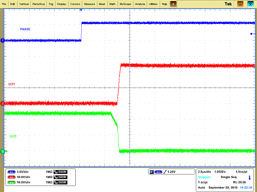
 Figure 8. Direction Change
 Figure 9. Current Limiting