SLVS912J January 2009 – January 2016 DRV8821
PRODUCTION DATA.
- 1 Features
- 2 Applications
- 3 Description
- 4 Revision History
- 5 Pin Configuration and Functions
- 6 Specifications
- 7 Detailed Description
- 8 Application and Implementation
- 9 Power Supply Recommendations
- 10Layout
- 11Device and Documentation Support
- 12Mechanical, Packaging, and Orderable Information
Package Options
Mechanical Data (Package|Pins)
- DCA|48
Thermal pad, mechanical data (Package|Pins)
- DCA|48
Orderable Information
7 Detailed Description
7.1 Overview
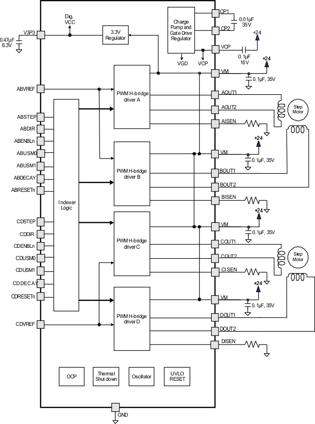
The DRV8821 is a dual stepper motor driver solution for applications that require independent control of two different motors. The device integrates four NMOS H-bridges, a microstepping indexer, and various fault protection features. The DRV8821 can be powered with a supply voltage between 8 and 32 V, and is capable of providing an output current up to 1.5-A full scale. Actual full-scale current will depend on ambient temperature, supply voltage, and PCB ground size.
A simple STEP/DIR interface allows easy interfacing to the controller circuit. The internal indexer is able to execute high-accuracy microstepping without requiring the processor to control the current level. The indexer is cable of full step and half step as well as microstepping to 1/4 and 1/8.
The current regulation is configurable with two different decay modes; slow decay and mixed decay. The mixed decay mode uses slow decay on increasing current steps and mixed decay on decreasing current steps, while slow decay mode will always use slow decay regardless increasing or decreasing steps.
The gate drive to each FET in all four H-Bridges is controlled to prevent any cross-conduction (shoot through current) during transitions.
7.2 Functional Block Diagram

7.3 Feature Description
7.3.1 PWM Motor Drivers
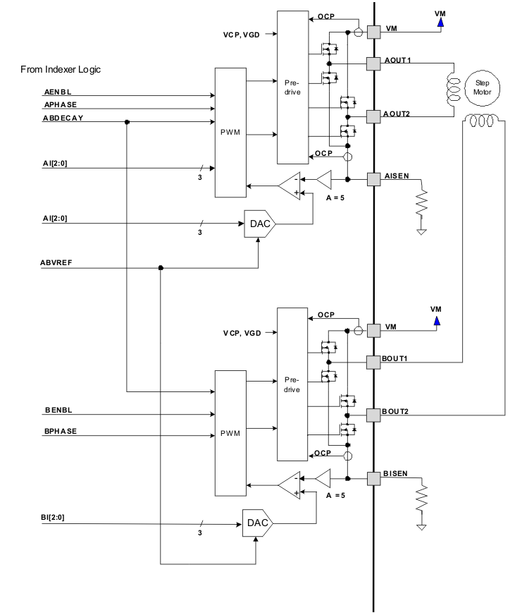
The DRV8821 contains four H-bridge motor drivers with current-control PWM circuitry. A block diagram showing drivers A and B of the motor control circuitry (as typically used to drive a bipolar stepper motor) is shown below. Drivers C and D are the same as A and B (though the Rds(on) of the output FETs is different).
 Figure 10. Block Diagram
Note that there are multiple VM motor power supply pins. All VM pins must be connected together to the motor supply voltage.
7.3.2 Current Regulation
The PWM chopping current is set by a comparator which compares the voltage across a current sense resistor connected to the xISEN pins, multiplied by a factor of 5, with a reference voltage. The reference voltage is input from the xVREF pin.
The full-scale (100%) chopping current is calculated as follows:

Example:
If a 0.5-Ω sense resistor is used and the VREFx pin is 2.5 V, the full-scale (100%) chopping current is
2.5 V/(5 × 0.5 Ω) = 1 A.
The reference voltage is also scaled by an internal DAC that allows torque control for fractional stepping of a bipolar stepper motor, as described in Microstepping Indexer.
7.3.3 Blanking Time
After the current is enabled in an H-bridge, the voltage on the xISEN pin is ignored for a fixed period of time before enabling the current sense circuitry. This blanking time is fixed at 3.75 μs. Note that the blanking time also sets the minimum on time of the PWM.
7.3.4 Microstepping Indexer
Built-in indexer logic in the DRV8821 allows a number of different stepping configurations. The xUSM1 and xUSM0 pins are used to configure the stepping format as shown in the table below:
Table 1. Microstepping Selection Bits
| xUSM1 | xUSM0 | STEP MODE |
|---|---|---|
| 0 | 0 | Full step (2-phase excitation) |
| 0 | 1 | ½ step (1-2 phase excitation) |
| 1 | 0 | 1/4 step (W1-2 phase excitation) |
| 1 | 1 | Eight microsteps/steps |
The following table shows the relative current and step directions for different settings of xUSM1 and xUSM0. At each rising edge of the xSTEP input, the indexer travels to the next state in the table. The direction is shown with the DIR pin high; if the xDIR pin is low the sequence is reversed. Positive current is defined as xOUT1 = positive with respect to xOUT2.
Note that the home state is 45 degrees. This state is entered at power-up, during sleep mode, or application of xRESETn.
Motor AB and motor CD act independently, and their indexer logic functions identically.
Table 2. Microstepping Indexer
| FULL STEP xUSM = 00 |
½ STEP xUSM = 01 |
1/4 STEP xUSM = 10 |
1/8 STEP xUSM = 11 |
AOUTx CURRENT (% FULL-SCALE) |
BOUTx CURRENT (% FULL-SCALE) |
STEP ANGLE (DEGREES) |
|---|---|---|---|---|---|---|
| 1 | 1 | 1 | 100 | 0 | 0 | |
| 2 | 98 | 20 | 11.25 | |||
| 2 | 3 | 92 | 38 | 22.5 | ||
| 4 | 83 | 56 | 33.75 | |||
| 1 | 2 | 3 | 5 | 71 | 71 | 45 (home state) |
| 6 | 56 | 83 | 56.25 | |||
| 4 | 7 | 38 | 92 | 67.5 | ||
| 8 | 20 | 98 | 78.75 | |||
| 3 | 5 | 9 | 0 | 100 | 90 | |
| 10 | –20 | 98 | 101.25 | |||
| 6 | 11 | –38 | 92 | 112.5 | ||
| 12 | –56 | 83 | 123.75 | |||
| 2 | 4 | 7 | 13 | –71 | 71 | 135 |
| 14 | –83 | 56 | 146.25 | |||
| 8 | 15 | –92 | 38 | 157.5 | ||
| 16 | –98 | 20 | 168.75 | |||
| 5 | 9 | 17 | –100 | 0 | 180 | |
| 18 | –98 | –20 | 191.25 | |||
| 10 | 19 | –92 | –38 | 202.5 | ||
| 20 | –83 | –56 | 213.75 | |||
| 3 | 6 | 11 | 21 | –71 | –71 | 225 |
| 22 | –56 | –83 | 236.25 | |||
| 12 | 23 | –38 | –92 | 247.5 | ||
| 24 | –20 | –98 | 258.75 | |||
| 7 | 13 | 25 | 0 | –100 | 270 | |
| 26 | 20 | –98 | 281.25 | |||
| 14 | 27 | 38 | –92 | 292.5 | ||
| 28 | 56 | –83 | 303.75 | |||
| 4 | 8 | 15 | 29 | 71 | –71 | 315 |
| 30 | 83 | –56 | 326.25 | |||
| 16 | 31 | 92 | –38 | 337.5 | ||
| 32 | 98 | –20 | 348.75 |
7.3.5 xRESETn and xENBLn Operation
The xRESETn pin, when driven active low, resets the step table to the home position. It also disables the H-bridge drivers. The xSTEP input is ignored while xRESETn is active. Note that there is a separate xRESETn pin for each motor; each acts only on one of the two motor controllers.
The xENABLEn pin is used to control the output drivers. When xENBLn is low, the output H-bridges are enabled. When xENBLn is high, the H-bridges are disabled and the outputs are in a high-impedance state.. Note that there is a separate xENBLn pin for each motor; each acts only on one of the two motor drivers.
Note that when xENBLn is high, the input pins and control logic, including the indexer (xSTEP and xDIR pins) are still functional.
Driving both ABENBLn and CDENBLn high will put the device into a low power sleep state. In this state, the H-bridges are disabled, both indexers are reset to the home state, the gate drive charge pump is stopped, and all internal clocks are stopped. In this state all inputs are ignored until one or both of the xENBLn pits return active low.
7.3.6 Protection Circuits
The DRV8821 is fully protected against undervoltage, overcurrent and overtemperature events.
7.3.6.1 Overcurrent Protection (OCP)
All of the drivers in DRV8821 are protected with an OCP (Over-Current Protection) circuit.
The OCP circuit includes an analog current limit circuit, which acts by removing the gate drive from each output FET if the current through it exceeds a preset level. This circuit will limit the current to a level that is safe to prevent damage to the FET.
A digital circuit monitors the analog current limit circuits. If any analog current limit condition exists for longer than a preset period, all drivers in the device will be disabled.
The device is re-enabled upon the removal and re-application of power at the VM pins.
7.3.6.2 Thermal Shutdown (TSD)
If the die temperature exceeds safe limits, all drivers in the device will be shut down.
The device will remain disabled until the die temperature has fallen to a safe level. After the temperature has fallen, the device may be re-enabled upon the removal and re-application of power at the VM pin.
7.3.6.3 Undervoltage Lockout (UVLO)
If at any time the voltage on the VM pins falls below the undervoltage lockout threshold voltage, all circuitry in the device will be disabled. Operation will resume when VM rises above the UVLO threshold. The indexer logic will be reset to its initial condition in the event of an undervoltage lockout.
7.3.6.4 Shoot-Through Current Prevention
The gate drive to each FET in the H-bridge is controlled to prevent any cross-conduction (shoot through current) during transitions.
7.4 Device Functional Modes
7.4.1 Decay Mode
The DRV8821 supports two different decay modes: slow decay or mixed decay. The mixed decay mode uses slow decay on increasing steps and mixed decay on decreasing steps. Mixed decay mode begins as fast decay but after a period of time (75% of the PWM cycle), switches to slow decay mode for the remainder of the fixed PWM period.
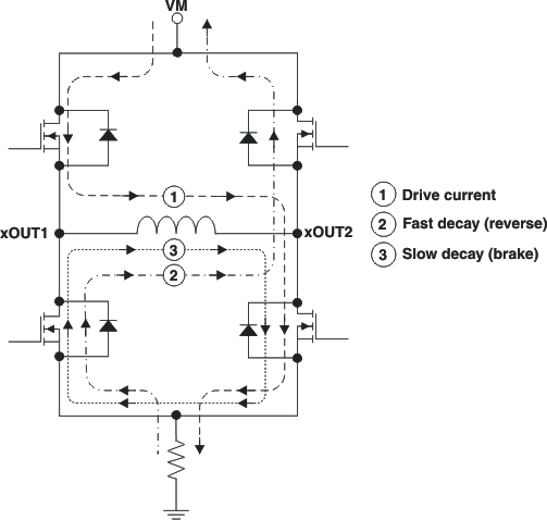
During PWM current chopping, the H-bridge is enabled to drive through the motor winding until the PWM current chopping threshold is reached. This is shown in Figure 11 as case 1. The current flow direction shown indicates positive current flow in Figure 11.
Once the chopping current threshold is reached, the H-bridge can operate in two different states, fast decay or slow decay.
In fast decay mode, once the PWM chopping current level has been reached, the H-bridge reverses state to allow winding current to flow in a reverse direction. As the winding current approaches zero, the bridge is disabled to prevent any reverse current flow. Fast-decay mode is shown in Figure 11 as case 2.
In slow-decay mode, winding current is re-circulated by enabling both of the low-side FETs in the bridge. This is shown in Figure 11 as case 3.
 Figure 11. Decay Mode
The DRV8821 also supports a mixed decay mode. Mixed decay mode begins as fast decay, but after a period of time (75% of the PWM cycle) switches to slow decay mode for the remainder of the fixed PWM period.
Mixed decay mode is only active if the current through the winding is decreasing (per the indexer step table); if the current is increasing, then slow decay is always used.
Slow or mixed decay mode is selected by the state of the xDECAY pins - logic low selects slow decay, and logic high selects mixed decay operation.