SLVS913E January 2009 – January 2016 DRV8823
PRODUCTION DATA.
- 1 Features
- 2 Applications
- 3 Description
- 4 Revision History
- 5 Pin Configuration and Functions
- 6 Specifications
- 7 Detailed Description
- 8 Application and Implementation
- 9 Power Supply Recommendations
- 10Layout
- 11Device and Documentation Support
- 12Mechanical, Packaging, and Orderable Information
Package Options
Mechanical Data (Package|Pins)
- DCA|48
Thermal pad, mechanical data (Package|Pins)
- DCA|48
Orderable Information
7 Detailed Description
7.1 Overview
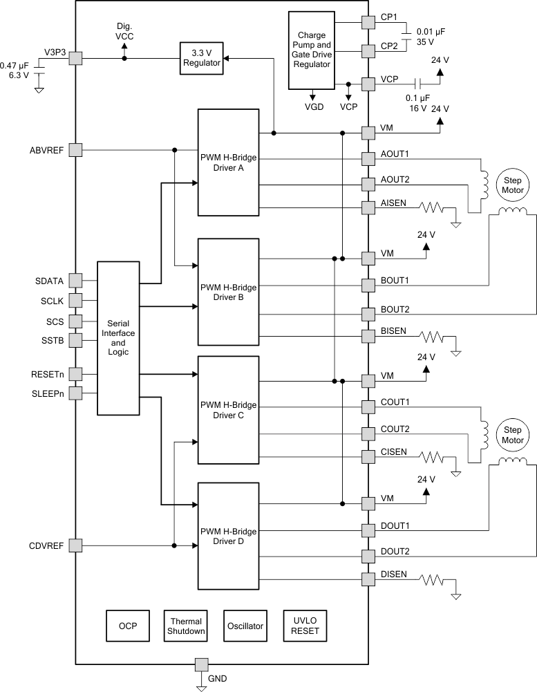
The DRV8823 is a dual stepper motor driver solution for applications that require independent control of two different motors. The device integrates four NMOS H-bridges, a microstepping indexer, and various fault protection features. The DRV8823 can be powered with a supply voltage between 8 and 32 V, and is capable of providing an output current up to 1.5 A full scale. Actual full-scale current will depend on ambient temperature, supply voltage and PCB ground size.
A serial data interface is included to control all functions of the motor driver. Current regulation through all four H-bridges is achieved using three register bits per H-bridge. The three register bits are used to scale the current in each bridge as a percentage of the full-scale current set by VREF input pin and sense resistor. The current regulation is configurable with two different decay modes, fixed slow and mixed.
The gate drive to each FET in all four H-Bridges is controlled to prevent any cross-conduction (shoot through current) during transitions.
7.2 Functional Block Diagram

7.3 Feature Description
7.3.1 PWM Motor Drivers
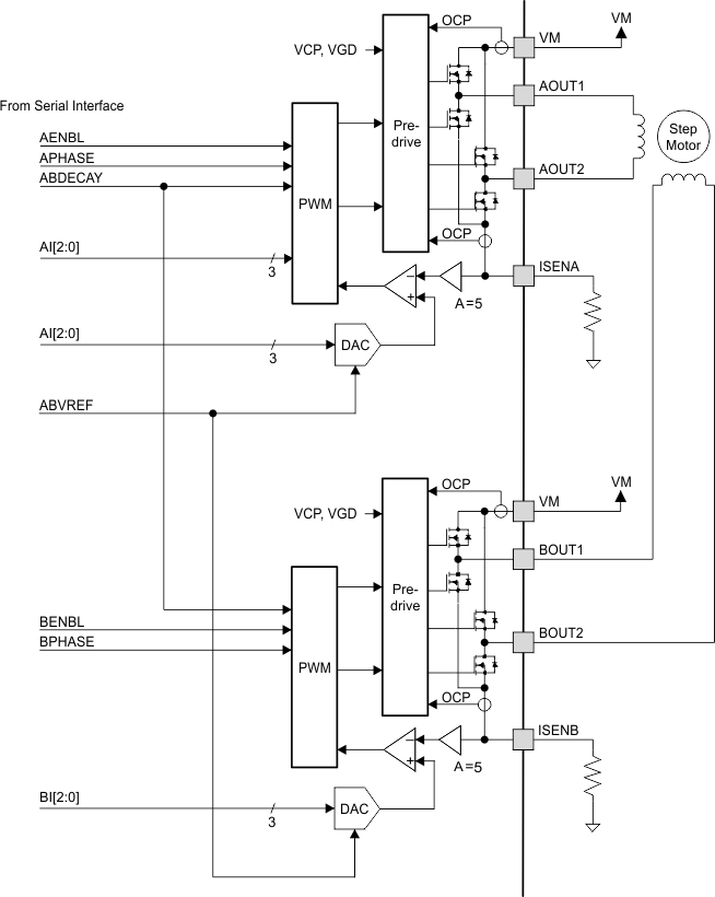
The DRV8823 contains four H-bridge motor drivers with current-control PWM circuitry. Figure 10 shows a block diagram with drivers A and B of the motor control circuitry (as typically used to drive a bipolar stepper motor). Drivers C and D are the same as A and B (though the RDS(ON) of the output FETs is different).
 Figure 10. Block Diagram With Drivers A and B
NOTE
The device has multiple VM motor power supply pins. All VM pins must be connected together to the motor supply voltage.
7.4 Device Functional Modes
 Figure 11. Logic Inputs
7.4.1 Bridge Control
The xENBL bits in the serial interface registers enable current flow in each H-bridge when set to 1.
The xPHASE bits in the serial interface registers control the direction of current flow through each H-bridge. Table 1 shows the logic.
Table 1. Bridge Control Logic
| xPHASE | xOUT1 | xOUT2 |
|---|---|---|
| 1 | H | L |
| 0 | L | H |
7.4.2 Current Regulation
The motor driver employs fixed-frequency PWM current regulation (also called current chopping). When a winding is activated, the current through it rises until it reaches a threshold, then the current is switched off until the next PWM period.
The PWM frequency is fixed at 50 kHz, but may also be set to 100 kHz by factory option.
The PWM chopping current is set by a comparator which compares the voltage across a current sense resistor connected to the xISEN pins, multiplied by a factor of 5, with a reference voltage. The reference voltage is input from the VREF pin.
The full-scale (100%) chopping current is calculated as follows:

Example:
If a 0.5-Ω sense resistor is used and the VREFx pin is 2.5 V, the full-scale (100%) chopping current is
2.5 V / (5 × 0.5 Ω) = 1 A.
Three serial interface register bits per H-bridge (xI2, xI1, and xI0) are used to scale the current in each bridge as a percentage of the full-scale current set by the VREF input pin and sense resistance. Table 2 shows the function of the bits.
Table 2. Bit Functions
| xI2 | xI1 | xI0 | Relative Current (% Full-Scale Chopping Current) |
|---|---|---|---|
| 0 | 0 | 0 | 20 |
| 0 | 0 | 1 | 38 |
| 0 | 1 | 0 | 56 |
| 0 | 1 | 1 | 71 |
| 1 | 0 | 0 | 83 |
| 1 | 0 | 1 | 92 |
| 1 | 1 | 0 | 98 |
| 1 | 1 | 1 | 100 |
7.4.3 Blanking Time
After the current is enabled in an H-bridge, the voltage on the xISEN pin is ignored for a fixed period of time before enabling the current sense circuitry. This blanking time is fixed at 3.75 μs. Note that the blanking time also sets the minimum on-time of the PWM.
7.4.4 Decay Mode
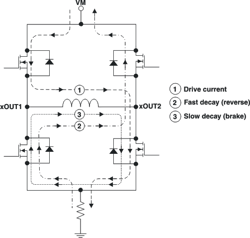
During PWM current chopping, the H-bridge is enabled to drive through the motor winding until the PWM current chopping threshold is reached (see case 1 in Figure 12). The current flow direction shown indicates positive current flow in Figure 12.
After the chopping current threshold is reached, the H-bridge can operate in two different states: fast decay or slow decay.
In fast-decay mode, after the PWM chopping current level is reached, the H-bridge reverses state to allow winding current to flow in a reverse direction. As the winding current approaches 0, the bridge is disabled to prevent any reverse current flow. See case 2 in Figure 12 for fast-decay mode.
In slow-decay mode, winding current is recirculated by enabling both of the low-side FETs in the bridge (see case 3 in Figure 12).
 Figure 12. Decay Mode
The DRV8823 supports slow decay and also a mixed-decay mode. Mixed-decay mode begins as fast decay, but at a fixed period of time (75% of the PWM cycle) it switches to slow decay mode for the remainder of the fixed PWM period.
The state of the xDECAY bits in the serial interface registers selects whether the device is in slow-decay or mixed-decay mode. If the xDECAY bit is 0,the device selects slow decay. If the xDECAY bit is 1, the device selects mixed decay.
7.4.5 Protection Circuits
The DRV8823 is fully protected against undervoltage, overcurrent, and overtemperature events.
7.4.5.1 OCP
All of the drivers in DRV8823 are protected with an OCP circuit.
The OCP circuit includes an analog current limit circuit, which acts by removing the gate drive from each output FET if the current through it exceeds a preset level. This circuit limits the current to a level that is safe to prevent damage to the FET.
A digital circuit monitors the analog current limit circuits. If any analog current limit condition exists for longer than a preset period, all drivers in the device are disabled.
The device is re-enabled upon the removal and re-application of power at the VM pins.
7.4.5.2 Thermal Shutdown (TSD)
If the die temperature exceeds safe limits, all drivers in the device are shut down.
The device remains disabled until the die temperature has fallen to a safe level. After the temperature has fallen, the device may be re-enabled upon the removal and re-application of power at the VM pin.
7.4.5.3 Undervoltage Lockout (UVLO)
If at any time the voltage on the VM pins falls below the UVLO threshold voltage, all circuitry in the device is disabled. Operation resumes when VM rises above the UVLO threshold. The indexer logic is reset to its initial condition in the event of an UVLO.
7.4.5.4 Shoot-Through Current Prevention
The gate drive to each FET in the H-bridge is controlled to prevent any cross-conduction (shoot through current) during transitions.
7.4.6 Serial Data Transmission
Data transfers consist of sixteen bits of serial data, shifted into the SDATA pin LSB first.
On serial writes to DRV8823, additional clock edges following the final data bit continue to shift data bits into the data register; therefore, the last 16 bits presented are latched and used.
Select one of two registers by setting bits in an address field in the four upper bits in the serial data transferred (ADDR in Table 3 and Table 4). One 16-bit register is used to control motor 1 (bridges A and B), and a second 16-bit register is used to control motor 2 (bridges C and D).
Data can only be transferred into the serial interface if the SCS input pin is active high.
Data is initially clocked into a temporary holding register. This data is latched into the motor driver on the rising edge of the SSTB pin. If the SSTB pin is tied high at all times, the data is latched in after all 16 bits have been transferred.
Programming
7.4.7 Data Format
Table 3. Motor 1 Command (Bridges A and B)
| Bit | D15:D12 | D11 | D10 | D9 | D8 | D7 | D6 | D5 | D4 | D3 | D2 | D1 | D0 |
|---|---|---|---|---|---|---|---|---|---|---|---|---|---|
| Name | ADDR (= 0000) |
BDECAY | B12 | B11 | B10 | BPHASE | BENBL | ADECAY | A12 | A11 | A10 | APHASE | AENBL |
| Reset Value | x | 0 | 0 | 0 | 0 | 0 | 0 | 0 | 0 | 0 | 0 | 0 | 0 |
Table 4. Motor 2 Command (Bridges C and D)
| Bit | D15:D12 | D11 | D10 | D9 | D8 | D7 | D6 | D5 | D4 | D3 | D2 | D1 | D0 |
|---|---|---|---|---|---|---|---|---|---|---|---|---|---|
| Name | ADDR (= 0001) |
DDECAY | D12 | D11 | D10 | DPHASE | DENBL | CDECAY | C12 | C11 | C10 | CPHASE | CENBL |
| Reset Value | x | 0 | 0 | 0 | 0 | 0 | 0 | 0 | 0 | 0 | 0 | 0 | 0 |
