SLVS913E January 2009 – January 2016 DRV8823
PRODUCTION DATA.
- 1 Features
- 2 Applications
- 3 Description
- 4 Revision History
- 5 Pin Configuration and Functions
- 6 Specifications
- 7 Detailed Description
- 8 Application and Implementation
- 9 Power Supply Recommendations
- 10Layout
- 11Device and Documentation Support
- 12Mechanical, Packaging, and Orderable Information
Package Options
Mechanical Data (Package|Pins)
- DCA|48
Thermal pad, mechanical data (Package|Pins)
- DCA|48
Orderable Information
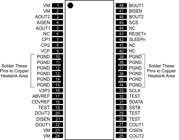
5 Pin Configuration and Functions
DCA Package
48-Pin HTSSOP
Top View

Pin Functions
| PIN | I/O(1) | DESCRIPTION | EXTERNAL COMPONENTS OR CONNECTIONS | |
|---|---|---|---|---|
| NAME | NO. | |||
| POWER AND GROUND | ||||
| VM | 1 | — | Motor supply voltage (multiple pins) | Connect all VM pins together to motor supply voltage. Bypass to GND with several 0.1-μF, 35-V ceramic capacitors. |
| 2 | ||||
| 23 | ||||
| 24 | ||||
| V3P3 | 16 | — | 3.3-V regulator output | Bypass to GND with 0.47-μF, 6.3-V ceramic capacitor. |
| GND | 10 to 15 | — | Power ground (multiple pins) | Connect all PGND pins to GND and solder to copper heatsink areas. |
| 34 to 39 | ||||
| CP1 | 7 | I/O | Charge pump flying capacitor | Connect a 0.01-μF capacitor between CP1 and CP2 |
| CP2 | 8 | I/O | ||
| VCP | 9 | I/O | Charge pump storage capacitor | Connect a 0.1-μF, 16-V ceramic capacitor to VM |
| MOTOR DRIVERS | ||||
| ABVREF | 17 | I | Bridge A and B current set reference voltage | Sets current trip threshold. |
| AOUT1 | 5 | O | Bridge A output 1 | Connect to first coil of bipolar stepper motor 1, or DC motor winding. |
| AOUT2 | 3 | O | Bridge A output 2 | |
| ISENA | 4 | — | Bridge A current sense | Connect to current sense resistor for bridge A. |
| BOUT1 | 48 | O | Bridge B output 1 | Connect to second coil of bipolar stepper motor 1, or DC motor winding. |
| BOUT2 | 46 | O | Bridge B output 2 | |
| ISENB | 47 | — | Bridge B current sense | Connect to current sense resistor for bridge B. |
| CDVREF | 18 | I | Bridge C and D current set reference voltage | Sets current trip threshold. |
| COUT1 | 27 | O | Bridge C output 1 | Connect to first coil of bipolar stepper motor 2, or DC motor winding. |
| COUT2 | 25 | O | Bridge C output 2 | |
| ISENC | 26 | — | Bridge C current sense | Connect to current sense resistor for bridge C. |
| DOUT1 | 22 | O | Bridge D output 1 | Connect to second coil of bipolar stepper motor 2, or DC motor winding. |
| DOUT2 | 20 | O | Bridge D output 2 | |
| ISEND | 22 | — | Bridge D current sense | Connect to current sense resistor for bridge D. |
| SERIAL INTERFACE | ||||
| SDATA | 31 | I | Serial data input | Data is clocked in on rising edge of SCLK. |
| SCLK | 33 | I | Serial input clock | Logic high enables serial data to be clocked in. |
| SCS | 45 | I | Serial chip select | Logic high latches serial data. |
| SSTB | 30 | I | Serial data strobe | Active low resets serial interface and disables outputs. |
| RESETn | 43 | I | Reset input | Active-low input disables outputs and charge pump. |
| SLEEPn | 42 | I | Sleep input | |
| TEST PINS | ||||
| TEST | 19 | I | Test inputs | Do not connect these pins (used for factory test only). |
| 28 | ||||
| 29 | ||||
| 32 | ||||
(1) Directions: I = Input, O = Output, OZ = Tri-state output, OD = Open-drain output, I/O = Input/output, PU = Internal pullup