SLVSA74E May 2010 – September 2015 DRV8829
PRODUCTION DATA.
- 1 Features
- 2 Applications
- 3 Description
- 4 Revision History
- 5 Pin Configuration and Functions
- 6 Specifications
- 7 Detailed Description
- 8 Application and Implementation
- 9 Power Supply Recommendations
- 10Layout
- 11Device and Documentation Support
- 12Mechanical, Packaging, and Orderable Information
Package Options
Mechanical Data (Package|Pins)
- PWP|28
Thermal pad, mechanical data (Package|Pins)
- PWP|28
Orderable Information
1 Features
- Single H-Bridge PWM Motor Driver
- Single Brushed-DC Motor Driver
- 1/2 Bipolar Stepper Motor Driver
- 5-A peak or 3.5-A rms Output Current
- 6.5- to 45-V Operating Supply Voltage Range
- Simple PH/EN Control Interface
- Multiple Decay Modes
- Mixed Decay
- Slow Decay
- Fast Decay
- Low-Current Sleep Mode (10 µA)
- Small Package and Footprint
- 28 HTSSOP (PowerPAD)
-
Protection Features
- VM Undervoltage Lockout (UVLO)
- Overcurrent Protection (OCP)
- Thermal Shutdown (TSD)
- Fault Condition Indication Pin (nFAULT)
2 Applications
- Automatic Teller and Money Handling Machines
- Video Security Cameras
- Multi-Function Printers and Scanners
- Office Automation Machines
- Gaming Machines
- Factory Automation and Robotics
- Stage Lighting Equipment
3 Description
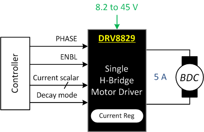
The DRV8829 is a brushed-DC motor or 1/2 bipolar stepper driver for industrial applications. The device output stage consists of an N-channel power MOSFET H-bridge driver. The DRV8829 is capable of driving up to 5-A peak current or 3.5-A rms current (with proper printed-circuit-board ground plane for thermal dissipation and at 24 V and TA = 25°C).
The PH/EN pins provide a simple control interface. An internal sense amplifier allows for adjustable current control. A low-power sleep mode is provided for very low quiescent current standby using a dedicated nSLEEP pin. Current regulation decay mode can be set to slow, fast, or mixed decay.
Internal protection functions are provided for undervoltage, overcurrent, short-circuits, and overtemperature. Fault conditions are indicated by a nFAULT pin.
Device Information(1)
| PART NUMBER | PACKAGE | BODY SIZE (NOM) |
|---|---|---|
| DRV8829 | HTSS0P (28) | 9.70 mm × 4.40 mm |
- For all available packages, see the orderable addendum at the end of the data sheet.
Simplified Schematic
