SLVSB18H March 2012 – August 2016 DRV8835
PRODUCTION DATA.
- 1 Features
- 2 Applications
- 3 Description
- 4 Revision History
- 5 Pin Configuration and Functions
- 6 Specifications
- 7 Detailed Description
- 8 Application and Implementation
- 9 Power Supply Recommendations
- 10Layout
- 11Device and Documentation Support
- 12Mechanical, Packaging, and Orderable Information
Package Options
Mechanical Data (Package|Pins)
- DSS|12
Thermal pad, mechanical data (Package|Pins)
- DSS|12
Orderable Information
6 Specifications
6.1 Absolute Maximum Ratings
See (1)(2)| MIN | MAX | UNIT | |||
|---|---|---|---|---|---|
| Power supply voltage, VM | –0.3 | 12 | V | ||
| Power supply voltage, VCC | –0.3 | 7 | V | ||
| Digital input pin voltage | –0.5 | VCC + 0.5 | V | ||
| Peak motor drive output current | Internally limited | A | |||
| Continuous motor drive output current per H-bridge(3) | –1.5 | 1.5 | A | ||
| TJ | Operating junction temperature | –40 | 150 | °C | |
| Tstg | Storage temperature | –60 | 150 | °C | |
(1) Stresses beyond those listed under Absolute Maximum Ratings may cause permanent damage to the device. These are stress ratings only, which do not imply functional operation of the device at these or any other conditions beyond those indicated under Recommended Operating Conditions. Exposure to absolute-maximum-rated conditions for extended periods may affect device reliability.
(2) All voltage values are with respect to network ground terminal.
(3) Power dissipation and thermal limits must be observed.
6.2 ESD Ratings
| VALUE | UNIT | |||
|---|---|---|---|---|
| V(ESD) | Electrostatic discharge | Human-body model (HBM), per ANSI/ESDA/JEDEC JS-001(1) | ±2000 | V |
| Charged-device model (CDM), per JEDEC specification JESD22-C101(2) | ±1500 | |||
(1) JEDEC document JEP155 states that 500-V HBM allows safe manufacturing with a standard ESD control process.
(2) JEDEC document JEP157 states that 250-V CDM allows safe manufacturing with a standard ESD control process.
6.3 Recommended Operating Conditions
TA = 25°C (unless otherwise noted)| MIN | NOM | MAX | UNIT | ||
|---|---|---|---|---|---|
| VCC | Device power supply voltage | 2 | 7 | V | |
| VM | Motor power supply voltage | 0 | 11 | V | |
| VIN | Logic level input voltage | 0 | VCC | V | |
| IOUT | H-bridge output current(1) | 0 | 1.5 | A | |
| ƒPWM | Externally applied PWM frequency | 0 | 250 | kHz | |
(1) Power dissipation and thermal limits must be observed.
6.4 Thermal Information
| THERMAL METRIC(1) | DRV8835 | UNIT | |
|---|---|---|---|
| DSS (WSON) | |||
| 12 PINS | |||
| RθJA | Junction-to-ambient thermal resistance | 50.4 | °C/W |
| RθJC(top) | Junction-to-case (top) thermal resistance | 58 | °C/W |
| RθJB | Junction-to-board thermal resistance | 19.9 | °C/W |
| ψJT | Junction-to-top characterization parameter | 0.9 | °C/W |
| ψJB | Junction-to-board characterization parameter | 20 | °C/W |
| RθJC(bot) | Junction-to-case (bottom) thermal resistance | 6.9 | °C/W |
(1) For more information about traditional and new thermal metrics, see the Semiconductor and IC Package Thermal Metrics application report.
6.5 Electrical Characteristics
TA = 25°C, VM = 5 V, VCC = 3 V (unless otherwise noted)6.6 Timing Requirements
TA = 25°C, VM = 5 V, VCC = 3 V, RL = 20 Ω| NO. | MIN | MAX | UNIT | ||
|---|---|---|---|---|---|
| 1 | t1 | Delay time, xPHASE high to xOUT1 low | 300 | ns | |
| 2 | t2 | Delay time, xPHASE high to xOUT2 high | 200 | ns | |
| 3 | t3 | Delay time, xPHASE low to xOUT1 high | 200 | ns | |
| 4 | t4 | Delay time, xPHASE low to xOUT2 low | 300 | ns | |
| 5 | t5 | Delay time, xENBL high to xOUTx high | 200 | ns | |
| 6 | t6 | Delay time, xENBL high to xOUTx low | 300 | ns | |
| 7 | t7 | Output enable time | 300 | ns | |
| 8 | t8 | Output disable time | 300 | ns | |
| 9 | t9 | Delay time, xINx high to xOUTx high | 160 | ns | |
| 10 | t10 | Delay time, xINx low to xOUTx low | 160 | ns | |
| 11 | tR | Output rise time | 30 | 188 | ns |
| 12 | tF | Output fall time | 30 | 188 | ns |
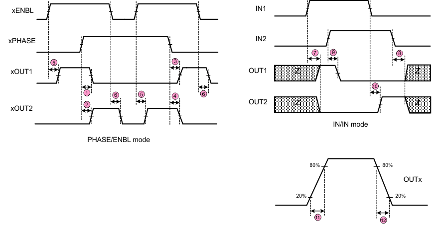 Figure 1. Timing Requirements
6.7 Typical Characteristics
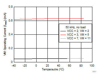 Figure 2. VM Operating Current
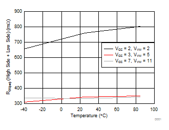 Figure 4. RDS(ON) (High-Side + Low-Side)
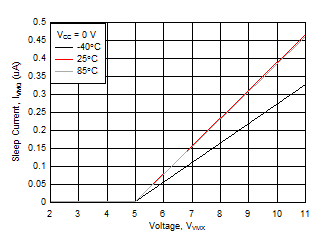 Figure 3. Sleep Current
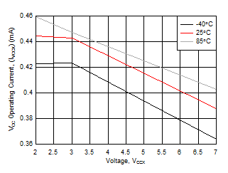 Figure 5. VCC Operating Current