SLVSET1 August   2018 DRV8873

PRODUCTION DATA.  

  1. Features
  2. Applications
  3. Description
    1.     Simplified Schematic
  4. Revision History
  5. Pin Configuration and Functions
    1.     Pin Functions
  6. Specifications
    1. 6.1 Absolute Maximum Ratings
    2. 6.2 ESD Ratings
    3. 6.3 Recommended Operating Conditions
    4. 6.4 Thermal Information
    5. 6.5 Electrical Characteristics
    6. 6.6 SPI Timing Requirements
    7. 6.7 Typical Characteristics
  7. Detailed Description
    1. 7.1 Overview
    2. 7.2 Functional Block Diagram
    3. 7.3 Feature Description
      1. 7.3.1 Bridge Control
        1. 7.3.1.1 Control Modes
        2. 7.3.1.2 Half-Bridge Operation
        3. 7.3.1.3 Internal Current Sense and Current Regulation
        4. 7.3.1.4 Slew-Rate Control
        5. 7.3.1.5 Dead Time
        6. 7.3.1.6 Propagation Delay
        7. 7.3.1.7 nFAULT Pin
        8. 7.3.1.8 nSLEEP as SDO Reference
      2. 7.3.2 Motor Driver Protection Circuits
        1. 7.3.2.1 VM Undervoltage Lockout (UVLO)
        2. 7.3.2.2 VCP Undervoltage Lockout (CPUV)
        3. 7.3.2.3 Overcurrent Protection (OCP)
          1. 7.3.2.3.1 Latched Shutdown (OCP_MODE = 00b)
          2. 7.3.2.3.2 Automatic Retry (OCP_MODE = 01b)
          3. 7.3.2.3.3 Report Only (OCP_MODE = 10b)
          4. 7.3.2.3.4 Disabled (OCP_MODE = 11b)
        4. 7.3.2.4 Open-Load Detection (OLD)
          1. 7.3.2.4.1 Open-Load Detection in Passive Mode (OLP)
          2. 7.3.2.4.2 Open-Load Detection in Active Mode (OLA)
        5. 7.3.2.5 Thermal Shutdown (TSD)
          1. 7.3.2.5.1 Latched Shutdown (TSD_MODE = 0b)
          2. 7.3.2.5.2 Automatic Recovery (TSD_MODE = 1b)
        6. 7.3.2.6 Thermal Warning (OTW)
      3. 7.3.3 Hardware Interface
        1. 7.3.3.1 MODE (Tri-Level Input)
        2. 7.3.3.2 Slew Rate
    4. 7.4 Device Functional Modes
      1. 7.4.1 Motor Driver Functional Modes
        1. 7.4.1.1 Sleep Mode (nSLEEP = 0)
        2. 7.4.1.2 Disable Mode (nSLEEP = 1, DISABLE = 1)
        3. 7.4.1.3 Operating Mode (nSLEEP = 1, DISABLE = 0)
        4. 7.4.1.4 nSLEEP Reset Pulse
    5. 7.5 Programming
      1. 7.5.1 Serial Peripheral Interface (SPI) Communication
        1. 7.5.1.1 SPI Format
        2. 7.5.1.2 SPI for a Single Slave Device
        3. 7.5.1.3 SPI for Multiple Slave Devices in Parallel Configuration
        4. 7.5.1.4 SPI for Multiple Slave Devices in Daisy Chain Configuration
    6. 7.6 Register Maps
      1. 7.6.1 Status Registers
        1. 7.6.1.1 FAULT Status Register Name (address = 0x00)
          1. Table 21. FAULT Status Register Field Descriptions
        2. 7.6.1.2 DIAG Status Register Name (address = 0x01)
          1. Table 22. DIAG Status Register Field Descriptions
      2. 7.6.2 Control Registers
        1. 7.6.2.1 IC1 Control Register (address = 0x02)
          1. Table 24. IC1 Control Register Field Descriptions
        2. 7.6.2.2 IC2 Control Register (address = 0x03)
          1. Table 25. IC2 Control Register Field Descriptions
        3. 7.6.2.3 IC3 Control Register (address = 0x04)
          1. Table 26. IC3 Control Register Field Descriptions
        4. 7.6.2.4 IC4 Control Register (address = 0x05)
          1. Table 27. IC4 Control Register Field Descriptions
  8. Application and Implementation
    1. 8.1 Application Information
    2. 8.2 Typical Application
      1. 8.2.1 Design Requirements
        1. 8.2.1.1 Motor Voltage
        2. 8.2.1.2 Drive Current and Power Dissipation
        3. 8.2.1.3 Sense Resistor
      2. 8.2.2 Detailed Design Procedure
        1. 8.2.2.1 Thermal Considerations
        2. 8.2.2.2 Heatsinking
      3. 8.2.3 Application Curves
  9. Power Supply Recommendations
    1. 9.1 Bulk Capacitance Sizing
  10. 10Layout
    1. 10.1 Layout Guidelines
    2. 10.2 Layout Example
  11. 11Device and Documentation Support
    1. 11.1 Documentation Support
      1. 11.1.1 Related Documentation
    2. 11.2 Receiving Notification of Documentation Updates
    3. 11.3 Community Resources
    4. 11.4 Trademarks
    5. 11.5 Electrostatic Discharge Caution
    6. 11.6 Glossary
  12. 12Mechanical, Packaging, and Orderable Information
    1. 12.1 Package Option Addendum
      1. 12.1.1 Packaging Information
      2. 12.1.2 Tape and Reel Information

Package Options

Mechanical Data (Package|Pins)
Thermal pad, mechanical data (Package|Pins)
Orderable Information

Open-Load Detection in Active Mode (OLA)

Open load in active mode is detected when the OUT1 and OUT2 voltages do not exhibit overshoot greater than the VOLA over VM between the time the low-side FET is switched off and the high-side FET is switched on during an output PWM cycle, as shown in Figure 20. An open load is not detected if the energy stored in the inductor is high enough to cause an overshoot greater than the VOLA over VM caused by the flyback current flowing through the body diode of the high-side FET. The OLA diagnostic is disabled by default and can be enabled by writing a 1b to the EN_OLA bit in IC4 control register.
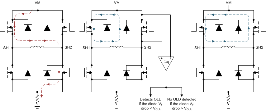
DRV8873 drv8873-q1-h-bridge-diode-hysteresis.gifFigure 20. Open-Load Active Mode Circuit

In PH/EN and PWM mode, the motor current decays by high-side recirculation. In independent PWM mode, the motor can enter the brake state either by high-side or low-side recirculation. If the motor enters the brake state using low-side recirculation, the diode VF voltage of high-side FET is less than the VOLA voltage which flags an open load fault even though the load is connected across the OUT1 and OUT2 pins. In this case, the OLA mode should not be used. If high-side current recirculation is done with independent PWM mode, the OLA mode functions properly.

NOTE

The OLA mode is functional only when high-side recirculation of the motor current occurs. Depending on the operation conditions and external circuitry, such as the output capacitors, an open load condition could be indicated even though the load is present. This case might occur, for example, during a direction change or for small load currents with respectively small PWM duty cycles. Therefore, TI recommends evaluating the open load diagnosis only in known, suitable operating conditions and to ignore it otherwise.

To avoid inadvertently triggering the open load diagnosis, a failure counter is implemented. Three consecutive occurrences of the internal open-load signal must occur, essentially three consecutive PWM pulses without freewheeling detected, before an open load condition is reported by the nFAULT pin and in the SPI register.

In the hardware version of the device, OLA mode is active when the nOL pin if left as a no-connect pin or tied to ground. If low-side current recirculation is done with independent PWM control, an open load condition is detected even though the load is connected. To avoid this false trip, the OLD must be disabled by taking the nOL pin high; however, both OLA and OLP diagnostics will be disabled.