SLVSDO1C January 2017 – March 2020 DRV8886AT
PRODUCTION DATA.
- 1 Features
- 2 Applications
- 3 Description
- 4 Revision History
- 5 Pin Configuration and Functions
- 6 Specifications
-
7 Detailed Description
- 7.1 Overview
- 7.2 Functional Block Diagram
- 7.3
Feature Description
- 7.3.1 Stepper Motor Driver Current Ratings
- 7.3.2 PWM Motor Drivers
- 7.3.3 Microstepping Indexer
- 7.3.4 Current Regulation
- 7.3.5 Controlling RREF With an MCU DAC
- 7.3.6 Decay Modes
- 7.3.7 Blanking Time
- 7.3.8 Charge Pump
- 7.3.9 Linear Voltage Regulators
- 7.3.10 Logic and Multi-Level Pin Diagrams
- 7.3.11 Protection Circuits
- 7.4 Device Functional Modes
- 8 Application and Implementation
- 9 Power Supply Recommendations
- 10Layout
- 11Device and Documentation Support
- 12Mechanical, Packaging, and Orderable Information
Package Options
Mechanical Data (Package|Pins)
Thermal pad, mechanical data (Package|Pins)
Orderable Information
7.3.5 Controlling RREF With an MCU DAC
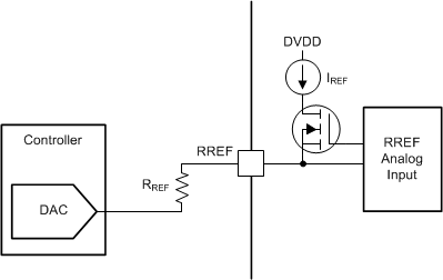
In some cases, the full-scale output current may need to be changed between many different values, depending on motor speed and loading. The reference current of the RREF pin can be adjusted in the system by tying the RREF resistor to a DAC output instead of GND.
In this mode of operation, as the DAC voltage increases, the reference current decreases and therefore the full-scale regulation current decreases as well. For proper operation, the output of the DAC should not rise above VRREF.
 Figure 15. Controlling RREF with a DAC Resource
 Use Equation 2 to calculate the full-scale regulation current as controlled by a controller DAC.

For example, if a 20-kΩ resistor is connected from the RREF pin to the DAC, and the DAC outputs 0.74 V, the chopping current is 600 mA (TRQ at 100%)
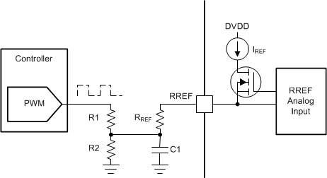
The RREF pin can also be adjusted using a PWM signal and low-pass filter.
 Figure 16. Controlling RREF With a PWM Resource