SNLS399B January 2012 – January 2015 DS100DF410
PRODUCTION DATA.
- 1 Features
- 2 Applications
- 3 Description
- 4 Revision History
- 5 Pin Configuration and Functions
- 6 Specifications
-
7 Detailed Description
- 7.1 Overview
- 7.2 Functional Block Diagram
- 7.3
Feature Description
- 7.3.1 Device Data Path Operation
- 7.3.2 Signal Detect
- 7.3.3 CTLE
- 7.3.4 DFE
- 7.3.5 Clock and Data Recovery
- 7.3.6 Output Driver
- 7.3.7 CTLE Boost Setting
- 7.3.8 DFE Tap Weight and Polarity Setting
- 7.3.9 Driver Output Voltage
- 7.3.10 Driver Output De-Emphasis
- 7.3.11 Driver Output Rise/Fall Time
- 7.3.12 Ref_mode 0 Mode (Reference Clock Not Required)
- 7.3.13 Ref_mode 3 Mode (Reference Clock Required)
- 7.3.14 False Lock Detector Setting
- 7.3.15 Reference Clock In
- 7.3.16 Reference Clock Out
- 7.3.17 Daisy Chain of REFCLK_OUT to REFCLK_IN
- 7.3.18 INT
- 7.3.19 LOCK_3, LOCK_2, LOCK_1, and LOCK_0
- 7.4 Device Functional Modes
- 7.5
Programming
- 7.5.1 SMBus Strap Observation
- 7.5.2 Device Revision and Device ID
- 7.5.3 Control/Shared Register Reset
- 7.5.4 Interrupt Channel Flag Bits
- 7.5.5 SMBus Master Mode Control Bits
- 7.5.6 Resetting Individual Channels of the Retimer
- 7.5.7 Interrupt Status
- 7.5.8 Overriding the CTLE Boost Setting
- 7.5.9 Overriding the VCO CAP DAC Values
- 7.5.10 Overriding the Output Multiplexer
- 7.5.11 Overriding the VCO Divider Selection
- 7.5.12 Using the PRBS Generator
- 7.5.13 Using the Internal Eye Opening Monitor
- 7.5.14 Overriding the DFE Tap Weights and Polarities
- 7.5.15 Enabling Slow Rise/Fall Time on the Output Driver
- 7.5.16 Inverting the Output Polarity
- 7.5.17 Overriding the Figure of Merit for Adaptation
- 7.5.18 Setting the Rate and Subrate for Lock Acquisition
- 7.5.19 Setting the Adaptation/Lock Mode
- 7.5.20 Initiating Adaptation
- 7.5.21 Setting the Reference Enable Mode
- 7.5.22 Overriding the CTLE Settings Used for CTLE Adaptation
- 7.5.23 Setting the Output Differential Voltage
- 7.5.24 Setting the Output De-emphasis Setting
- 7.6 Register Maps
- 8 Application and Implementation
- 9 Power Supply Recommendations
- 10Layout
- 11Device and Documentation Support
- 12Mechanical, Packaging, and Orderable Information
Package Options
Mechanical Data (Package|Pins)
- RHS|48
Thermal pad, mechanical data (Package|Pins)
- RHS|48
Orderable Information
8 Application and Implementation
NOTE
Information in the following applications sections is not part of the TI component specification, and TI does not warrant its accuracy or completeness. TI’s customers are responsible for determining suitability of components for their purposes. Customers should validate and test their design implementation to confirm system functionality.
8.1 Application Information
The DS100DF410 can be configured by the user to optimize its operation. The four channels can be optimized independently in SMBus master or SMBus slave mode. The operational settings available for user configuration include the following.
- CTLE boost setting
- DFE tap weight and polarity setting
- Driver output voltage
- Driver output de-emphasis
- Driver output rise/fall time
Configuration of the DS100DF410 is accomplished by writing the appropriate values into various device registers over the SMBus. This can either be done while the device is operating or upon initial power-up. When the DS100DF410 is operating it behaves like an SMBus slave device, and its register contents can be read or written over the SMBus. Optionally, when the DS100DF410 first powers up, it can behave like an SMBus master and read its register contents autonomously from an external EEPROM.
8.2 Typical Application
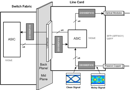 Figure 6. Typical Application Diagram
8.2.1 Design Requirements
This section lists some critical areas for high speed printed circuit board design consideration and study.
- Utilize 100-Ω differential impedance traces.
- Back-drill connector vias and signal vias to minimize stub length.
- Use reference plane vias to ensure a low inductance path for the return current.
- Place AC-Coupling capacitors for the transmitter links near the receiver for that channel.
- The maximum body size for AC-coupling capacitors is 0402.
8.2.2 Detailed Design Procedure
To begin the design process, determine the following:
- Maximum power draw for PCB regulator selection. For this calculation use the maximum transient power supply current specified in the datasheet. The lock time for each channel is typically very short, so this power calculation should not be used for the thermal simulations of the PCB.
- Maximum operational power for thermal calculations. For this calculation use the Average Power Consumption number in the datasheet.
- Select a reference clock frequency and routing scheme.
- Plan out channel connectivity. Be sure to note any desired polarity inversion routing in the board schematics.
- Ensure that each device has a unique SMBus address if the control bus is shared with other devices or components.
- Use the IBIS-AMI model for simple channel simulations before PCB layout is complete.
8.2.3 Application Curves
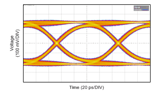
Figure 7 shows a typical output eye diagram for the DS100DF410 operating at 10.3125 Gbps with default VOD of 600mVp-p and de-emphasis setting of -2dB.
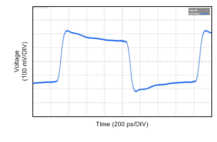
Figure 8 shows an example of Tx de-emphasis for a DS100DF410 operating at 10.3125 Gbps. In this example, the high speed output is configured for 600mVp-p VOD and de-emphasis is set to -4.5dB. An 8T pattern is used to evaluate the driver, which consists of 0xFF00.