SNLS482B April 2014 – January 2017 DS125DF1610
PRODUCTION DATA.
- 1 Features
- 2 Applications
- 3 Description
- 4 Revision History
- 5 Pin Configuration and Functions
- 6 Specifications
-
7 Detailed Description
- 7.1 Overview
- 7.2 Functional Block Diagram
- 7.3
Feature Description
- 7.3.1 Device Data Path Operation
- 7.3.2 AC-Coupled Receiver with Signal Detect
- 7.3.3 CTLE
- 7.3.4 Cross Point Switch
- 7.3.5 DFE with VGA
- 7.3.6 Clock and Data Recovery
- 7.3.7 Reference Clock
- 7.3.8 Differential Driver with FIR Filter
- 7.3.9 Setting the Output VOD
- 7.3.10 Output Driver Polarity Inversion
- 7.3.11 Driver Output Rise/Fall Time
- 7.3.12 Debug Features
- 7.3.13 Interrupt Signals
- 7.3.14 Other Features
- 7.4 Device Functional Modes
- 7.5 Programming
- 8 Application and Implementation
- 9 Power Supply Recommendations
- 10Layout
- 11Device and Documentation Support
- 12Mechanical, Packaging, and Orderable Information
Package Options
Mechanical Data (Package|Pins)
- ABB|196
Thermal pad, mechanical data (Package|Pins)
Orderable Information
1 Features
- Pin-Compatible Family
- DS150DF1610: 12.5 to 15 G
- DS125DF1610: 9.8 to 12.5 G
- DS110DF1610: 8.5 to 11.3 G
- 4x4 Analog Cross Point Switch for Each Quad
- Fully Adaptive CTLE
- Self tuning DFE, with Optional Continuous Adaption
- Configurable VGA
- Adjustable Transmit VOD
- Adjustable 3-tap Transmit FIR Filter
- On-chip AC Coupling on Receive Inputs
- Locks to Half/Quarter/Eighth Data Rates for Legacy Support
- On-chip Eye Monitor(EOM), PRBS Checker, Pattern Generator
- Supports JTAG Boundary Scan
- Programmable Output Polarity Inversion
- Input Signal Detection, CDR Lock Detection
- Single 2.5 V ±5% Power Supply
- SMBus Based Register Configuration
- Optional EEPROM Configuration
- 15 mm × 15 mm, 196-pin FCBGA Package
- Operating Temp Range : –40°C to +85°C
2 Applications
- SFF-8431
- CPRI
- 10G/40G Ethernet
- Backplanes
3 Description
The DS125DF1610 is a sixteen-channel multi-rate retimer with integrated signal conditioning features. The device includes a fully adaptive Continuous Time Linear Equalizer (CTLE), Decision Feedback Equalizer (DFE), clock and data recovery (CDR), and a transmit FIR filter to enhance the reach and robustness over long, lossy, crosstalk impaired high speed serial links to achieve BER < 1×10-15.
Each channel of the DS125DF1610 independently locks to serial data at 9.8 to 12.5 Gbps and the divide by 2, 4 and 8 sub-multiples. A simple external oscillator (±100ppm) that is synchronous or asynchronous with the incoming data stream is used as a reference clock. Integrated 4x4 cross point switches allow for full non-blocking routing or broadcasting within each quad of the DS125DF1610.
Programmable transmit FIR filter offers control of the pre-cursor, main tap and post-cursor for transmit equalization. The fully adaptive receive equalization (CTLE and DFE) enables longer distance transmission in lossy copper interconnects and backplanes with multiple connectors.
A non-disruptive mission mode eye-monitor feature allows link monitoring internal to the receiver. The built-in PRBS generator and checker compliment the internal diagnostic features to complete standalone BERT measurements. Built-in JTAG enables manufacturing tests.
Device Information (1)
| PART NUMBER | PACKAGE | BODY SIZE NOM |
|---|---|---|
| DS125DF1610 | FCBGA (196) | 15.00 mm x 15.00 mm |
- For all available packages, see the orderable addendum at the end of the datasheet
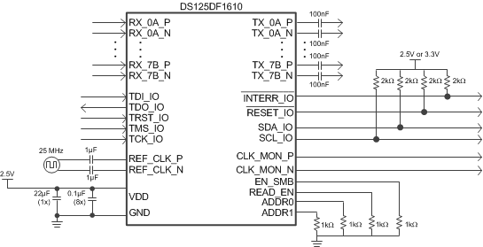
Simplified Schematic
