SNLS433C November 2012 – January 2015 DS90UH927Q-Q1
PRODUCTION DATA.
- 1 Features
- 2 Applications
- 3 Description
- 4 Revision History
- 5 Pin Configuration and Functions
-
6 Specifications
- 6.1 Absolute Maximum Ratings
- 6.2 ESD Ratings
- 6.3 Recommended Operating Conditions
- 6.4 Thermal Information
- 6.5 DC Electrical Characteristics
- 6.6 AC Electrical Characteristics
- 6.7 DC and AC Serial Control Bus Characteristics
- 6.8 Recommended Timing Requirements for the Serial Control Bus
- 6.9 Timing Requirements
- 6.10 Typical Characteristics
-
7 Detailed Description
- 7.1 Overview
- 7.2 Functional Block Diagram
- 7.3
Feature Description
- 7.3.1 High-Speed Forward Channel Data Transfer
- 7.3.2 Low-Speed Back Channel Data Transfer
- 7.3.3 Common Mode Filter Pin (CMF)
- 7.3.4 Video Control Signals
- 7.3.5 EMI Reduction Features
- 7.3.6 Built-In Self Test (BIST)
- 7.3.7 Forward Channel and Back Channel Error Checking
- 7.3.8 Internal Pattern Generation
- 7.3.9 Remote Auto Power Down Mode
- 7.3.10 Input RxCLKIN Loss Detect
- 7.3.11 Serial Link Fault Detect
- 7.3.12 INTERRUPT Pin (INTB)
- 7.3.13 General-Purpose I/O
- 7.3.14 I2S Audio Interface
- 7.3.15 Additional Features
- 7.4 Device Functional Modes
- 7.5 Programming
- 7.6 Register Maps
- 8 Application and Implementation
- 9 Power Supply Recommendations
- 10Layout
- 11Device and Documentation Support
- 12Mechanical, Packaging, and Orderable Information
Package Options
Mechanical Data (Package|Pins)
- RTA|40
Thermal pad, mechanical data (Package|Pins)
- RTA|40
Orderable Information
7 Detailed Description
7.1 Overview
The DS90UH927Q-Q1 converts a FPD-Link interface (4 LVDS data channels + 1 LVDS Clock) to a FPD-Link III interface. This device transmits a 35-bit symbol over a single serial pair operating at up to a 2.975-Gbps line rate. The serial stream contains an embedded clock, video control signals, RGB video data, and audio data. The payload is DC-balanced to enhance signal quality and support AC coupling.
The DS90UH927Q-Q1 applies encryption to the video data using a High-Bandwidth Digital Content Protection (HDCP) Cipher, and transmits the encrypted data out through the FPD-Link III interface. Audio encryption is supported. On chip non-volatile memory stores the HDCP keys. All key exchanges are conducted over the FPD-Link III bidirectional control interface.
The DS90UH927Q-Q1 serializer is intended for use with a DS90UH928Q-Q1 or DS90UH926Q-Q1 deserializer, but is also backward compatible with DS90UR906Q, DS90UR908Q, DS90UR910Q, and DS90UR916Q FPD-Link II deserializers.
The DS90UH927Q-Q1 serializer and DS90UH928Q-Q1 or DS90UH926Q-Q1 deserializer incorporate an I2C compatible interface. The I2C compatible interface allows programming of serializer or deserializer devices from a local host controller. In addition, the devices incorporate a bidirectional control channel (BCC) that allows communication between serializer/deserializer as well as remote I2C slave devices.
The bidirectional control channel (BCC) is implemented via embedded signaling in the high-speed forward channel (serializer to deserializer) combined with lower speed signaling in the reverse channel (deserializer to serializer). Through this interface, the BCC provides a mechanism to bridge I2C transactions across the serial link from one I2C bus to another. The implementation allows for arbitration with other I2C compatible masters at either side of the serial link.
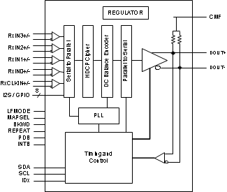
7.2 Functional Block Diagram
7.3 Feature Description
7.3.1 High-Speed Forward Channel Data Transfer
The High-Speed Forward Channel is composed of a 35-bit frame containing RGB data, sync signals, HDCP, I2C, and I2S audio transmitted from Serializer to Deserializer. Figure 13 illustrates the serial stream generated per PCLK cycle into RxCLKIN±. This data payload is optimized for signal transmission over an AC coupled link. Data is randomized, DC-balanced and scrambled.
 Figure 13. FPD-Link III Serial Stream
The device supports pixel clock ranges of 5 MHz to 15 MHz (LFMODE=1) and 15 MHz to 85 MHz (LFMODE=0). This corresponds to an application payload rate range of 155 Mbps to 2.635 Gbps, with an actual line rate range of 525 Mbps to 2.975 Gbps.
7.3.2 Low-Speed Back Channel Data Transfer
The Low-Speed Back Channel of the DS90UH927Q-Q1 provides bidirectional communication between the display and host processor. Data is transferred simultaneously over the same physical link as the high-speed forward channel data. The back channel transports I2C, HDCP, CRC, and 4 bits of standard GPIO information with a 10 Mbps line rate.
7.3.3 Common Mode Filter Pin (CMF)
The serializer provides access to the center tap of the internal CML termination. A 0.1-μF capacitor must be connected from this pin to GND for additional common-mode filtering of the differential pair (Figure 29). This increases noise rejection capability in high-noise environments.
7.3.4 Video Control Signals
The video control signal bits embedded in the high-speed FPD-Link LVDS are subject to certain limitations relative to the video pixel clock period (PCLK). By default, the DS90UH927Q-Q1 applies a minimum pulse width filter on these signals to help eliminate spurious transitions.
Normal Mode Control Signals (VS, HS, DE) have the following restrictions:
- Horizontal Sync (HS): The video control signal pulse width must be 3 PCLKs or longer when the Control Signal Filter (register bit 0x03[4]) is enabled (default). Disabling the Control Signal Filter removes this restriction (minimum is 1 PCLK). See Table 5. HS can have at most two transitions per 130 PCLKs.
- Vertical Sync (VS): The video control signal pulse is limited to 1 transition per 130 PCLKs. Thus, the minimum pulse width is 130 PCLKs.
- Data Enable Input (DE): The video control signal pulse width must be 3 PCLKs or longer when the Control Signal Filter (register bit 0x03[4]) is enabled (default). Disabling the Control Signal Filter removes this restriction (minimum is 1 PCLK). See Table 5. DE can have at most two transitions per 130 PCLKs.
7.3.5 EMI Reduction Features
7.3.5.1 LVCMOS VDDIO Option
The 1.8-V or 3.3-V LVCMOS inputs and outputs are powered from separate VDDIO supply pins to offer compatibility with external system interface signals. Note: When configuring the VDDIO power supplies, all the single-ended control input pins for device need to scale together with the same operating VDDIO levels. If VDDIO is selected to operate in the 3.0 V to 3.6 V range, VDDIO must be operated within 300 mV of VDD33.
7.3.6 Built-In Self Test (BIST)
An optional At-Speed Built-In Self Test (BIST) feature supports testing of the high speed serial link and the low-speed back channel without external data connections. This is useful in the prototype stage, equipment production, in-system test, and system diagnostics.
7.3.6.1 BIST Configuration and Status
The BIST mode is enabled at the deserializer by pin (BISTEN) or BIST configuration register. The test may select either an external PCLK or the 33 MHz internal Oscillator clock (OSC) frequency. In the absence of PCLK, the user can select the internal OSC frequency at the deserializer through the BISTC pin or BIST configuration register.
When BIST is activated at the deserializer, a BIST enable signal is sent to the serializer through the Back Channel. The serializer outputs a test pattern and drives the link at speed. The deserializer detects the test pattern and monitors it for errors. The deserializer PASS output pin toggles to flag each frame received containing one or more errors. The serializer also tracks errors indicated by the CRC fields in each back channel frame.
The BIST status can be monitored real time on the deserializer PASS pin, with each detected error resulting in a half pixel clock period toggled LOW. After BIST is deactivated, the result of the last test is held on the PASS output until reset (new BIST or Power Down). A high on PASS indicates NO ERRORS were detected. A Low on PASS indicates one or more errors were detected. The duration of the test is controlled by the pulse width applied to the deserializer BISTEN pin. LOCK status is valid throughout the entire duration of BIST.
See Figure 14 for the BIST mode flow diagram.
Sample BIST Sequence
Step 1: For the DS90UH927Q-Q1 paired with a FPD-Link III Deserializer, BIST Mode is enabled via the BISTEN pin of Deserializer. The desired clock source is selected through the deserializer BISTC pin.
Step 2: The DS90UH927Q-Q1 serializer is awakened through the back channel if it is not already on. An all-zeros pattern is balanced, scrambled, randomized, and sent through the FPD-Link III interface to the deserializer. Once the serializer and the deserializer are in BIST mode and the deserializer acquires Lock, the PASS pin of the deserializer goes high and BIST starts checking the data stream. If an error in the payload (1 to 35) is detected, the PASS pin will switch low for one half of the clock period. During the BIST, the PASS output can be monitored and counted to determine the payload error rate.
Step 3: To Stop the BIST mode, the deserializer BISTEN pin is set Low. The deserializer stops checking the data. The final test result is held on the PASS pin. If the test ran error free, the PASS output will remain HIGH. If there one or more errors were detected, the PASS output will output constant LOW. The PASS output state is held until a new BIST is run, the device is RESET, or the device is powered down. BIST duration is user-controlled and may be of any length.
The link returns to normal operation after the deserializer BISTEN pin is low. Figure 15 shows the waveform diagram of a typical BIST for two cases. Case 1 is error free, and Case 2 shows one with multiple errors. In most cases it is difficult to generate errors due to the robustness of the link (differential data transmission, and so forth), thus they may be introduced by greatly extending the cable length, faulting the interconnect medium, or reducing signal condition enhancements (Rx Equalization).
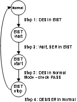 Figure 14. BIST Mode Flow Diagram
7.3.7 Forward Channel and Back Channel Error Checking
While in BIST mode, the serializer stops sampling the FPD-Link input pins and switches over to an internal all zeroes pattern. The internal all-zeroes pattern goes through scrambler, DC-balancing, and so forth, and is transmitted over the serial link to the deserializer. The deserializer, on locking to the serial stream, compares the recovered serial stream with all-zeroes and records any errors in status registers. Errors are also dynamically reported on the PASS pin of the deserializer.
The back-channel data is checked for CRC errors once the serializer locks onto the back-channel serial stream, as indicated by link detect status (register bit 0x0C[0] - Table 5). CRC errors are recorded in an 8-bit register in the serializer. The register is cleared when the serializer enters the BIST mode. As soon as the serializer enters BIST mode, the functional mode CRC register starts recording any back channel CRC errors. The BIST mode CRC error register is active in BIST mode only and keeps the record of the last BIST run until cleared or the serializer enters BIST mode again.
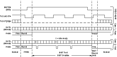 Figure 15. BIST Waveforms
7.3.8 Internal Pattern Generation
The DS90UH927Q-Q1 serializer provides an internal pattern generation feature. It allows basic testing and debugging of an integrated panel. The test patterns are simple and repetitive and allow for a quick visual verification of panel operation. As long as the device is not in power down mode, the test pattern will be displayed even if no input is applied. If no clock is received, the test pattern can be configured to use a programmed oscillator frequency. For detailed information, refer to Application Note AN-2198 Exploring the Internal Test Pattern Generation Feature of 720p (SNLA132).
7.3.8.1 Pattern Options
The DS90UH927Q-Q1 serializer pattern generator is capable of generating 17 default patterns for use in basic testing and debugging of panels. Each pattern can be inverted using register bits (Table 5). The 17 default patterns are listed as follows:
- White/Black (default/inverted)
- Black/White
- Red/Cyan
- Green/Magenta
- Blue/Yellow
- Horizontally Scaled Black to White/White to Black
- Horizontally Scaled Black to Red/Cyan to White
- Horizontally Scaled Black to Green/Magenta to White
- Horizontally Scaled Black to Blue/Yellow to White
- Vertically Scaled Black to White/White to Black
- Vertically Scaled Black to Red/Cyan to White
- Vertically Scaled Black to Green/Magenta to White
- Vertically Scaled Black to Blue/Yellow to White
- Custom Color (or its inversion) configured in PGRS
- Black-White/White-Black Checkerboard (or custom checkerboard color, configured in PGCTL)
- YCBR/RBCY VCOM pattern, orientation is configurable from PGCTL
- Color Bars (White, Yellow, Cyan, Green, Magenta, Red, Blue, Black) – Note: not included in the auto-scrolling feature
Additionally, the Pattern Generator incorporates one user-configurable full-screen 24-bit color, which is controlled by the PGRS, PGGS, and PGBS registers. This is pattern #14. One of the pattern options is statically selected in the PGCTL register when Auto-Scrolling is disabled. The PGTSC and PGTSO1-8 registers control the pattern selection and order when Auto-Scrolling is enabled.
7.3.8.2 Color Modes
By default, the Pattern Generator operates in 24-bit color mode, where all bits of the Red, Green, and Blue outputs are enabled. 18-bit color mode can be activated from the configuration registers (Table 5). In 18-bit mode, the 6 most significant bits (bits 7-2) of the Red, Green, and Blue outputs are enabled; the 2 least significant bits will be 0.
7.3.8.3 Video Timing Modes
The Pattern Generator has two video timing modes – external and internal. In external timing mode, the Pattern Generator detects the video frame timing present on the DE and VS inputs. If Vertical Sync signaling is not present on VS, the Pattern Generator determines Vertical Blank by detecting when the number of inactive pixel clocks (DE = 0) exceeds twice the detected active line length. In internal timing mode, the Pattern Generator uses custom video timing as configured in the control registers. The internal timing generation may also be driven by an external clock. By default, external timing mode is enabled. Internal timing or Internal timing with External Clock are enabled by the control registers (Table 5).
7.3.8.4 External Timing
In external timing mode, the Pattern Generator passes the incoming DE, HS, and VS signals unmodified to the video control outputs after a two pixel clock delay. It extracts the active frame dimensions from the incoming signals in order to properly scale the brightness patterns. If the incoming video stream does not use the VS signal, the Pattern Generator determines the Vertical Blank time by detecting a long period of pixel clocks without DE asserted.
7.3.8.5 Pattern Inversion
The Pattern Generator also incorporates a global inversion control, located in the PGCFG register, which causes the output pattern to be bitwise-inverted. For example, the full screen Red pattern becomes full-screen cyan, and the Vertically Scaled Black to Green pattern becomes Vertically Scaled White to Magenta.
7.3.8.6 Auto Scrolling
The Pattern Generator supports an Auto-Scrolling mode, in which the output pattern cycles through a list of enabled pattern types. A sequence of up to 16 patterns may be defined in the registers. The patterns may appear in any order in the sequence and may also appear more than once.
7.3.9 Remote Auto Power Down Mode
The DS90UH927Q-Q1 serializer features a Remote Auto Power Down mode. This feature is enabled and disabled through the register bit 0x01[7] (Table 5). When the back channel is not detected, either due to an idle or powered-down deserializer, the serializer enters remote auto power down mode. Power dissipation of the serializer is significantly reduced in this mode. The serializer automatically attempts to resume normal operation upon detection of an active back channel from the deserializer. To complete the wake-up process and reactivate forward channel operation, the remote power-down feature must be disabled by either a local I2C host, or by an auto-ACK I2C transaction from a remote I2C host located at the deserializer. The Remote Auto Power Down Sleep/Wake cycle is shown below in Figure 16:
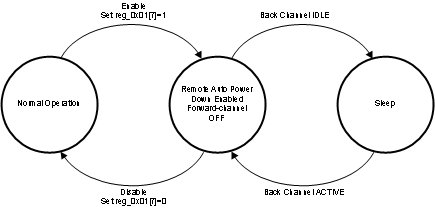 Figure 16. Remote Auto Power Down Sleep/Wake Cycle
To resume normal operation, the Remote Auto Power Down feature must be disabled in the device control register. This may be accomplished from a local I2C controller by writing reg_0x01[7]=0 (Table 5). To disable from a remote I2C controller located at the deserializer, perform the following procedure to complete the wake-up process:
- Power up remote deserializer (back channel must be active)
- Enable I2C PASS-THROUGH ALL by setting deserializer register reg_0x05[7]=1
- Enable I2C AUTO ACK by setting deserializer register reg_0x03[2]=1
- Disable Remote Auto Power Down by setting serializer register reg_0x01[7]=0
- Disable I2C AUTO ACK by setting deserializer register reg_0x03[2]=0
- Disable I2C PASS-THROUGH ALL by setting deserializer register reg_0x05[7]=0
7.3.10 Input RxCLKIN Loss Detect
The serializer can be programmed to enter a low power SLEEP state when the input clock (PCLK) is lost. A clock loss condition is detected when PCLK drops below approximately 1MHz. When a PCLK is detected again, the serializer will then lock to the incoming RxCLKIN±. Note: when RxCLKIN± is lost, the optional Serial Bus Control Registers values are still retained. See (Table 5) for more information.
7.3.11 Serial Link Fault Detect
The DS90UH927Q-Q1 can detect fault conditions in the FPD-Link III interconnect. If a fault condition occurs, the Link Detect Status is 0 (cable is not detected) on bit 0 of address 0x0C (Table 5). The DS90UH927Q-Q1 will detect any of the following conditions:
- Cable open
- + to - short
- + to GND short
- - to GND short
- + to battery short
- - to battery short
- Cable is linked incorrectly (DOUT+/DOUT- connections reversed)
NOTE
The device will detect any of the above conditions, but does not report specifically which one has occurred.
7.3.12 INTERRUPT Pin (INTB)
- On the DS90UH927Q-Q1 serializer, set register reg_0xC6[5] = 1 and 0xC6[0] = 1 (Table 5) to configure the interrupt.
- On the serializer, read from HDCP_ISR register 0xC7 to arm the interrupt for the first time.
- When INTB_IN on the deserializer (DS90UH926Q-Q1 or DS90UH928Q-Q1) is set LOW, the INTB pin on the serializer also pulls low, indicating an interrupt condition.
- The external controller detects INTB = LOW and reads the HDCP_ISR register (Table 5) to determine the interrupt source. Reading this register also clears and resets the interrupt.
7.3.13 General-Purpose I/O
7.3.13.1 GPIO[3:0]
In normal operation, GPIO[3:0] may be used as general purpose IOs in either forward channel (inputs) or back channel (outputs) applications. GPIO modes may be configured from the registers (Table 5). GPIO[1:0] are dedicated pins and GPIO[3:2] are shared with I2S_DC and I2S_DD respectively. Note: if the DS90UH927Q-Q1 is paired with a DS90UH926Q-Q1 deserializer, the devices must be configured into 18-bit mode to allow usage of GPIO pins on the DS90UH927 serializer. To enable 18-bit mode, set serializer register reg_0x12[2] = 1. 18-bit mode will be auto-loaded into the deserializer from the serializer. See Table 1 for GPIO enable and configuration.
Table 1. GPIO Enable and Configuration
| DESCRIPTION | DEVICE | FORWARD CHANNEL | BACK CHANNEL |
|---|---|---|---|
| GPIO3 | DS90UH927Q-Q1 | 0x0F = 0x03 | 0x0F = 0x05 |
| DS90UH926/8Q-Q1 | 0x1F = 0x05 | 0x1F = 0x03 | |
| GPIO2 | DS90UH927Q-Q1 | 0x0E = 0x30 | 0x0E = 0x50 |
| DS90UH926/8Q-Q1 | 0x1E = 0x50 | 0x1E = 0x30 | |
| GPIO1 | DS90UH927Q-Q1 | 0x0E = 0x03 | 0x0E = 0x05 |
| DS90UH926/8Q-Q1 | 0x1E = 0x05 | 0x1E = 0x03 | |
| GPIO0 | DS90UH927Q-Q1 | 0x0D = 0x03 | 0x0D = 0x05 |
| DS90UH926/8Q-Q1 | 0x1D = 0x05 | 0x1D = 0x03 |
The input value present on GPIO[3:0] may also be read from register, or configured to local output mode (Table 5).
7.3.13.2 GPIO[8:5]
GPIO_REG[8:5] are register-only GPIOs and may be programmed as outputs or read as inputs through local register bits only. Where applicable, these bits are shared with I2S pins and will override I2S input if enabled into REG_GPIO mode. See Table 2 for GPIO enable and configuration.
Note: Local GPIO value may be configured and read either through local register access, or remote register access through the Low-Speed Bidirectional Control Channel. Configuration and state of these pins are not transported from serializer to deserializer as is the case for GPIO[3:0].
Table 2. GPIO_REG and GPIO Local Enable and Configuration
| DESCRIPTION | REGISTER CONFIGURATION | FUNCTION |
|---|---|---|
| GPIO_REG8 | 0x11 = 0x01 | Output, L |
| 0x11 = 0x09 | Output, H | |
| 0x11 = 0x03 | Input, Read: 0x1D[0] | |
| GPIO_REG7 | 0x10 = 0x01 | Output, L |
| 0x10 = 0x09 | Output, H | |
| 0x10 = 0x03 | Input, Read: 0x1C[7] | |
| GPIO_REG6 | 0x10 = 0x01 | Output, L |
| 0x10 = 0x09 | Output, H | |
| 0x10 = 0x03 | Input, Read: 0x1C[6] | |
| GPIO_REG5 | 0x0F = 0x01 | Output, L |
| 0x0F = 0x09 | Output, H | |
| 0x0F = 0x03 | Input, Read: 0x1C[5] | |
| GPIO3 | 0x0F = 0x01 | Output, L |
| 0x0F = 0x09 | Output, H | |
| 0x0F = 0x03 | Input, Read: 0x1C[3] | |
| GPIO2 | 0x0E = 0x01 | Output, L |
| 0x0E = 0x09 | Output, H | |
| 0x0E = 0x03 | Input, Read: 0x1C[2] | |
| GPIO1 | 0x0E = 0x01 | Output, L |
| 0x0E = 0x09 | Output, H | |
| 0x0E = 0x03 | Input, Read: 0x1C[1] | |
| GPIO0 | 0x0D = 0x01 | Output, L |
| 0x0D = 0x09 | Output, H | |
| 0x0D = 0x03 | Input, Read: 0x1C[0] |
7.3.14 I2S Audio Interface
The DS90UH927Q-Q1 serializer features six I2S input pins that, when paired with a DS90UH928Q-Q1 deserializer, supports surround sound audio applications. The bit clock (I2S_CLK) supports frequencies between 1 MHz and the smaller of <PCLK/2 or <13 MHz. Four I2S data inputs transport two channels of I2S-formatted digital audio each, with each channel delineated by the word select (I2C_WC) input. I2S audio transport is not available in Backwards Compatibility Mode (BKWD = 1).
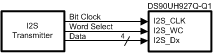 Figure 17. I2S Connection Diagram
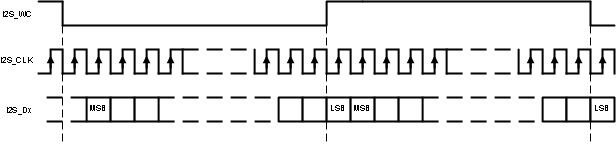 Figure 18. I2S Frame Timing Diagram
When paired with a DS90UH926Q-Q1, the DS90UH927Q-Q1 I2S interface supports a single I2S data input through I2S_DA (24-bit video mode), or two I2S data inputs through I2S_DA and I2S_DB (18-bit video mode).
Table 3 covers several common I2S sample rates:
Table 3. Audio Interface Frequencies
| Sample Rate (kHz) | I2S Data Word Size (bits) | I2S CLK (MHz) |
|---|---|---|
| 32 | 16 | 1.024 |
| 44.1 | 16 | 1.411 |
| 48 | 16 | 1.536 |
| 96 | 16 | 3.072 |
| 192 | 16 | 6.144 |
| 32 | 24 | 1.536 |
| 44.1 | 24 | 2.117 |
| 48 | 24 | 2.304 |
| 96 | 24 | 4.608 |
| 192 | 24 | 9.216 |
| 32 | 32 | 2.048 |
| 44.1 | 32 | 2.822 |
| 48 | 32 | 3.072 |
| 96 | 32 | 6.144 |
| 192 | 32 | 12.288 |
7.3.14.1 I2S Transport Modes
By default, audio is packetized and transmitted during video blanking periods in dedicated Data Island Transport frames. Data Island frames may be disabled from control registers if Forward Channel Frame Transport of I2S data is desired. In this mode, only I2S_DA is transmitted to the DS90UH928Q-Q1 deserializer. If connected to a DS90UH926Q-Q1 deserializer, I2S_DA and I2S_DB are transmitted. Surround Sound Mode, which transmits all four I2S data inputs (I2S_D[A..D]), may only be operated in Data Island Transport mode. This mode is only available when connected to a DS90UH928Q-Q1 deserializer.
7.3.14.2 I2S Repeater
I2S audio may be fanned-out and propagated in the repeater application. By default, data is propagated via Data Island Transport on the FPD-Link interface during the video blanking periods. If frame transport is desired, then the I2S pins should be connected from the deserializer to all serializers. Activating surround sound at the top-level deserializer automatically configures downstream DS90UH927Q-Q1 serializers and DS90UH928Q-Q1 deserializers for surround sound transport utilizing Data Island Transport. If 4-channel operation utilizing I2S_DA and I2S_DB only is desired, this mode must be explicitly set in each serializer and deserializer control register throughout the repeater tree (Table 5).
A DS90UH927Q-Q1 serializer configured in repeater mode may also regenerate I2S audio from its I2S input pins in lieu of Data Island frames. See the HDCP Repeater Connection Diagram (Figure 23) and the I2C Control Registers (Table 5) for additional details.
7.3.15 Additional Features
Additional pattern generator features can be accessed through the Pattern Generator Indirect Register Map. It consists of the Pattern Generator Indirect Address (PGIA reg_0x66 — Table 5) and the Pattern Generator Indirect Data (PGID reg_0x67 — Table 5). See Application Note AN-2198 Exploring the Internal Test Pattern Generation Feature of 720p (SNLA132).
7.4 Device Functional Modes
7.4.1 Power Down (PDB)
The Serializer has a PDB input pin to ENABLE or POWER DOWN the device. This pin may be controlled by an external device, or through VDDIO, where VDDIO = 3.0 V to 3.6 V or VDD33. To save power, disable the link when the display is not needed (PDB = LOW). Ensure that this pin is not driven HIGH before VDD33 and VDDIO have reached final levels. When PDB is driven low, ensure that the pin is driven to 0 V for at least 1.5 ms before releasing or driving high. In the case where PDB is pulled up to VDDIO = 3.0 V to 3.6 V or VDD33 directly, a 10-kΩ pullup resistor and a >10-µF capacitor to ground are required (See Figure 29).
Toggling PDB low will POWER DOWN the device and RESET all control registers to default. During this time, PDB must be held low for a minimum period of time. See AC Electrical Characteristics for more information.
7.4.2 Backward Compatible Mode
The DS90UH927Q-Q1 is also backward compatible to DS90UR906Q, DS90UR908Q FPD, and DS90UR916Q FPD-Link II deserializers for PCLK frequencies ranging from 5 MHz to 65 MHz. It is also backward compatible with the DS90UR910Q for PCLK frequencies ranging from 5 MHz to 75 MHz. The serializer transmits 28-bits of data over a single serial FPD-Link II pair operating at a payload rate of 120 Mbps to 1.8 Gbps, corresponding to a line rate of 140 Mbps to 2.1 Gbps. The Backward Compatibility configuration can be selected through the BKWD pin or programmed through the configuration register (Table 5). The bidirectional control channel, HDCP, bidirectional GPIOs, I2S, and interrupt (INTB) are not active in this mode. However, local I2C access to the serializer is still available. Note: PCLK frequency range in this mode is 15 MHz to 75 MHz for LFMODE=0 and 5 MHZ to <15 MHz for LFMODE=1.
7.4.3 Low Frequency Optimization (LFMODE)
The LFMODE is set via register (Table 5) or LFMODE Pin. This mode optimizes device operation for lower input data clock ranges supported by the serializer. If LFMODE is Low (LFMODE = 0, default), the RxCLKIN± frequency is between 15 MHz and 85 MHz. If LFMODE is High (LFMODE = 1), the RxCLKIN± frequency is between 5 MHz and <15 MHz. Note: when the device LFMODE is changed, a PDB reset is required. When LFMODE is high (LFMODE=1), the line rate relative to the input data rate is multiplied by four. Thus, for the operating range of 5 MHz to <15 MHz, the line rate is 700 Mbps to <2.1 Gbps with an effective data payload of 175 Mbps to 525 Mbps. Note: for Backwards Compatibility Mode (BKWD=1), the line rate relative to the input data rate remains the same.
7.4.4 FPD-Link Input Frame and Color Bit Mapping Select
The DS90UH927Q-Q1 can be configured to accept 24-bit color (8-bit RGB) with 2 different mapping schemes: LSBs on RxIN[3]±, shown in Figure 19, or MSBs on RxIN[3], shown in Figure 20. Each frame corresponds to a single pixel clock (PCLK) cycle. The LVDS clock input to RxCLKIN± follows a 4:3 duty cycle scheme, with each 28-bit pixel frame starting with two LVDS bit clock periods high, three low, and ending with two high. The mapping scheme is controlled by MAPSEL pin or by Register (Table 5).
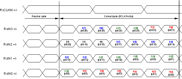 Figure 19. FPD-Link Mapping: LSBs on RxIN3 (MAPSEL=L)
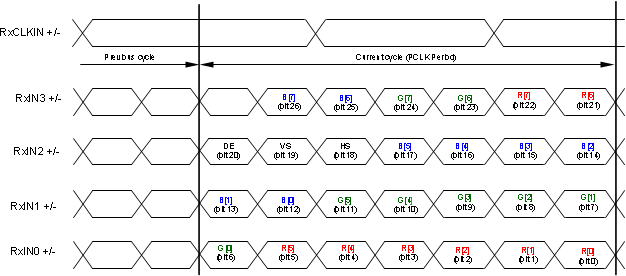 Figure 20. FPD-Link Mapping: MSBs on RxIN3 (MAPSEL=H)
7.4.5 HDCP
The Cipher function is implemented in the serializer per HDCP v1.3 specification. The DS90UH927Q-Q1 provides HDCP encryption of audiovisual content when connected to an HDCP capable FPD-Link III deserializer. HDCP authentication and shared key generation is performed using the HDCP Control Channel which is embedded in the forward and backward channels of the serial link. On-chip Non-Volatile Memory (NVM) is used to store the HDCP keys. The confidential HDCP keys are loaded by TI during the manufacturing process and are not accessible external to the device.
The DS90UH927Q-Q1 uses the Cipher engine to encrypt the data as per HDCP v1.3. The encrypted data is sent through the FPD-Link III interface.
7.4.5.1 HDCP Repeater
The supported HDCP Repeater application provides a mechanism to extend HDCP transmission over multiple links to multiple display devices. It authenticates all HDCP Receivers in the system and distributes protected content to the HDCP Receivers using the encryption mechanisms provided in the HDCP specification.
7.4.5.2 HDCP I2S Audio Encryption
When HDCP is active, packetized Data Island Transport audio is also encrypted along with the video data per HDCP v.1.3. I2S audio transmitted in Forward Channel Frame Transport mode is not encrypted. Depending on the quality and specifications of the audiovisual source, HDCP encryption of digital audio may be required. System designers should consult the specific HDCP specifications to determine if encryption of digital audio is required by the specific application audiovisual source.
7.4.5.3 Repeater Configuration
In HDCP repeater application, this document refers to the DS90UH927Q-Q1 as the HDCP Transmitter (TX), and refers to the DS90UH928Q-Q1 as the HDCP Receiver (RX). Figure 21 shows the maximum configuration supported for HDCP Repeater implementations using the DS90UH925/7Q-Q1 (TX), and DS90UH926/8Q-Q1 (RX). Two levels of HDCP Repeaters are supported with a maximum of three HDCP Transmitters per HDCP Receiver. To ensure parallel video interface compatibility, repeater nodes should feature either the DS90UH926Q-Q1/DS90UH925Q (RX/TX) chipset or the DS90UH927Q-Q1/DS90UH928Q-Q1 (TX/RX) chipset.
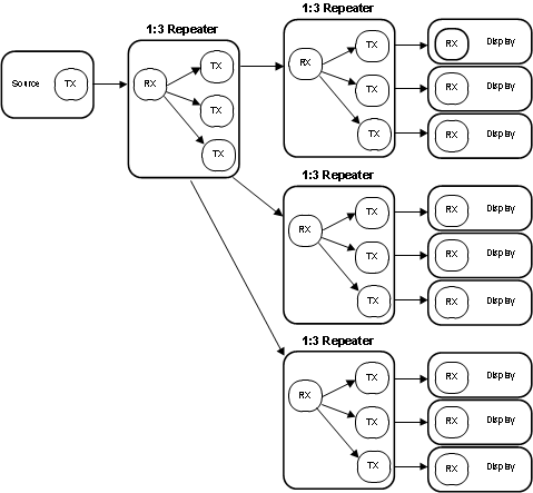 Figure 21. HDCP Maximum Repeater Application
In a repeater application, the I2C interface at each TX and RX may be configured to transparently pass I2C communications upstream or downstream to any I2C device within the system. This includes a mechanism for assigning alternate IDs (Slave Aliases) to downstream devices in the case of duplicate addresses.
To support HDCP Repeater operation, the RX includes the ability to control the downstream authentication process, assemble the KSV list for downstream HDCP Receivers, and pass the KSV list to the upstream HDCP Transmitter. An I2C master within the RX communicates with the I2C slave within the TX. The TX handles authenticating with a downstream HDCP Receiver and makes status available through the I2C interface. The RX monitors the transmit port status for each TX and reads downstream KSV and KSV list values from the TX.
In addition to the I2C interface used to control the authentication process, the HDCP Repeater implementation includes two other interfaces. The FPD-Link LVDS interface provides the unencrypted video data in 24-bit RGB format and includes the DE/VS/HS control signals. In addition to providing the RGB video data, the LVDS interface communicates control information and packetized audio data during video blanking intervals. A separate I2S audio interface may optionally be used to send I2S audio data between the HDCP Receiver and HDCP Transmitter in place of using the packetized audio. All audio and video data is decrypted at the output of the HDCP Receiver and is re-encrypted by the HDCP Transmitter. Figure 22 provides more detailed block diagram of a 1:2 HDCP repeater configuration.
If video data is output to a local display, White Balancing and Hi-FRC dithering functions should not be used as they will block encrypted I2S audio.
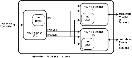 Figure 22. HDCP 1:2 Repeater Configuration
7.4.5.4 Repeater Connections
The HDCP Repeater requires the following connections between the HDCP Receiver and each HDCP Transmitter Figure 23.
- Video Data – Connect all FPD-Link data and clock pairs
- I2C – Connect SCL and SDA signals. Both signals should be pulled up to VDD33 or VDDIO = 3.0 V to 3.6 V with 4.7-kΩ resistors.
- Audio (optional) – Connect I2S_CLK, I2S_WC, and I2S_Dx signals.
- IDx pin – Each HDCP Transmitter and Receiver must have a unique I2C address.
- REPEAT pin — All HDCP Transmitters and Receivers must be set into Repeater Mode.
- Interrupt pin – Connect DS90UH928Q-Q1 INTB_IN pin to DS90UH927Q-Q1 INTB pin. The signal must be pulled up to VDDIO.
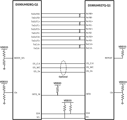 Figure 23. HDCP Repeater Connection Diagram
7.4.5.4.1 Repeater Fan-Out Electrical Requirements
Repeater applications requiring fan-out from one DS90UH928Q-Q1 deserializer to up to three DS90UH927Q-Q1 serializers requires special considerations for routing and termination of the FPD-Link differential traces. Figure 24 details the requirements that must be met for each signal pair:
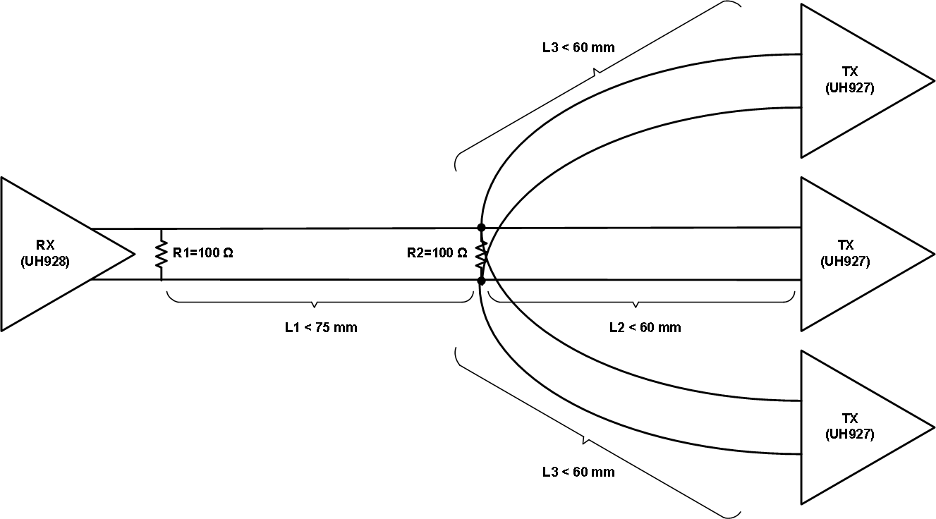 Figure 24. FPD-Link Fan-Out Electrical Requirements
7.5 Programming
7.5.1 Serial Control Bus
The DS90UH927Q-Q1 may also be configured by the use of an I2C compatible serial control bus. Multiple devices may share the serial control bus (up to 10 device addresses supported). The device address is set via a resistor divider (R1 and R2 — see Figure 25) connected to the IDx pin.
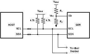 Figure 25. Serial Control Bus Connection
The serial control bus consists of two signals, SCL and SDA. SCL is a Serial Bus Clock Input. SDA is the Serial Bus Data Input / Output signal. Both SCL and SDA signals require an external pullup resistor to VDD33 or VDDIO = 3.0 V to 3.6 V. For most applications, a 4.7-kΩ pullup resistor to VDD33 is recommended. However, the pullup resistor value may be adjusted for capacitive loading and data rate requirements. The signals are either pulled High, or driven Low.
The IDx pin configures the control interface to one of 10 possible device addresses. A pullup resistor and a pulldown resistor may be used to set the appropriate voltage ratio between the IDx input pin (VR2) and VDD33, each ratio corresponding to a specific device address. See Table 5.
Table 4. Serial Control Bus Addresses for IDx
| # | Ideal Ratio VR2 / VDD33 |
Ideal VR2
(V) |
Suggested Resistor R1 kΩ (1% tol) | Suggested Resistor R2 kΩ (1% tol) | Address 7'b | Address 8'b |
|---|---|---|---|---|---|---|
| 1 | 0 | 0 | Open | 40.2 or >10 | 0x0C | 0x18 |
| 2 | 0.306 | 1.011 | 221 | 97.6 | 0x13 | 0x26 |
| 3 | 0.350 | 1.154 | 210 | 113 | 0x14 | 0x28 |
| 4 | 0.393 | 1.298 | 196 | 127 | 0x15 | 0x2A |
| 5 | 0.440 | 1.452 | 182 | 143 | 0x16 | 0x2C |
| 6 | 0.483 | 1.594 | 169 | 158 | 0x17 | 0x2E |
| 7 | 0.529 | 1.745 | 147 | 165 | 0x18 | 0x30 |
| 8 | 0.572 | 1.887 | 143 | 191 | 0x19 | 0x32 |
| 9 | 0.618 | 2.040 | 121 | 196 | 0x1A | 0x34 |
| 10 | 0.768 | 2.535 | 90.9 | 301 | 0x1B | 0x36 |
The Serial Bus protocol is controlled by START, START-Repeated, and STOP phases. A START occurs when SCL transitions Low while SDA is High. A STOP occurs when SDA transitions High while SCL is also HIGH. See Figure 26.
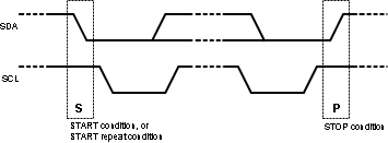 Figure 26. START and STOP Conditions
To communicate with a remote device, the host controller (master) sends the slave address and listens for a response from the slave. This response is referred to as an acknowledge bit (ACK). If a slave on the bus is addressed correctly, it Acknowledges (ACKs) the master by driving the SDA bus low. If the address doesn't match a device's slave address, it Not-acknowledges (NACKs) the master by letting SDA be pulled High. ACKs also occur on the bus when data is being transmitted. When the master is writing data, the slave ACKs after every data byte is successfully received. When the master is reading data, the master ACKs after every data byte is received to let the slave know it wants to receive another data byte. When the master wants to stop reading, it NACKs after the last data byte and creates a stop condition on the bus. All communication on the bus begins with either a Start condition or a Repeated Start condition. All communication on the bus ends with a Stop condition. A READ is shown in Figure 27 and a WRITE is shown in Figure 28.
 Figure 27. Serial Control Bus — READ
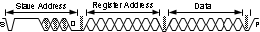 Figure 28. Serial Control Bus — WRITE
The I2C Master located at the DS90UH927Q-Q1 serializer must support I2C clock stretching. For more information on I2C interface requirements and throughput considerations, please refer to I2C Communication Over FPD-Link III with Bidirectional Control Channel (SNLA131).
7.6 Register Maps
Table 5. Serial Control Bus Registers
| ADD (dec) |
ADD (hex) |
Register Name | Bit | Register Type |
Default (hex) |
Function | Description |
|---|---|---|---|---|---|---|---|
| 0 | 0x00 | I2C Device ID | 7:1 | RW | IDx | Device ID | 7–bit address of Serializer Note: Read-only unless bit 0 is set |
| 0 | RW | ID Setting | I2C ID Setting 0: Device ID is from IDx pin 1: Register I2C Device ID overrides IDx pin |
||||
| 1 | 0x01 | Reset | 7 | RW | 0x00 | Remote Auto Power Down | Remote Auto Power Down 0: Do not power down when no Bidirectional Control Channel link is detected (default) 1: Enable power down when no Bidirectional Control Channel link is detected |
| 6:2 | Reserved. | ||||||
| 1 | RW | Digital RESET1 | Reset the entire digital block including registers This bit is self-clearing. 0: Normal operation (default) 1: Reset |
||||
| 0 | RW | Digital RESET0 | Reset the entire digital block except registers This bit is self-clearing 0: Normal operation (default) 1: Reset |
||||
| 3 | 0x03 | General Configuration | 7 | RW | 0xD2 | Back channel CRC Checker Enable | Back Channel Check Enable 0: Disable 1: Enable (default) |
| 6 | Reserved. | ||||||
| 5 | RW | I2C Remote Write Auto Acknowledge | Automatically Acknowledge I2C Remote Write When enabled, I2C writes to the Deserializer (or any remote I2C Slave, if I2C PASS ALL is enabled) are immediately acknowledged without waiting for the Deserializer to acknowledge the write. This allows higher throughput on the I2C bus. Note: this mode will prevent any NACK or read/write error indication from a remote device from reaching the I2C master. 0: Disable (default) 1: Enable |
||||
| 4 | RW | Filter Enable | HS, VS, DE two clock filter When enabled, pulses less than two full PCLK cycles on the DE, HS, and VS inputs will be rejected 0: Filtering disable 1: Filtering enable (default) |
||||
| 3 | RW | I2C Pass-through | I2C Pass-Through Mode Read/Write transactions matching any entry in the DeviceAlias registers will be passed through to the remote deserializer I2C interface. 0: Pass-Through Disabled (default) 1: Pass-Through Enabled |
||||
| 2 | Reserved | ||||||
| 1 | RW | PCLK Auto | Switch over to internal OSC in the absence of PCLK 0: Disable auto-switch 1: Enable auto-switch (default) |
||||
| 0 | RW | TRFB | Reserved | ||||
| 4 | 0x04 | Mode Select | 7 | RW | 0x80 | Failsafe State | Input Failsafe State 0: Failsafe to High 1: Failsafe to Low (default) |
| 6 | Reserved | ||||||
| 5 | RW | CRC Error Reset | Clear back channel CRC Error Counters This bit is NOT self-clearing 0: Normal Operation (default) 1: Clear Counters |
||||
| 4 | Reserved | ||||||
| 3 | RW | BKWD ModeOverride | Backward Compatible mode set by BKWD pin or register 0: BC mode is set by BKWD pin (default) 1: BC mode is set by register bit |
||||
| 2 | RW | BKWD | Backward compatibility mode, device to pair with DS90UR906Q, DS90UR908Q, or DS90UR916Q 0: Normal HDCP device (default) 1: Compatible with 906/908/916 |
||||
| 1 | RW | LFMODE Override | Frequency mode set by LFMODE pin or register 0: Frequency mode is set by LFMODE pin (default) 1: Frequency mode is set by register bit |
||||
| 0 | RW | LFMODE | Frequency mode select 0: High frequency mode (15 MHz ≤ RxCLKIN ≤ 85 MHz) (default) 1: Low frequency mode (5 MHz ≤ RxCLKIN < 15 MHz) |
||||
| 5 | 0x05 | I2C Control | 7:5 | 0x00 | Reserved | ||
| 4:3 | RW | SDA Output Delay | SDA output delay Configures output delay on the SDA output. Setting this value will increase output delay in units of 40 ns. Nominal output delay values for SCL to SDA are: 00: 240 ns (default) 01: 280 ns 10: 320 ns 11: 360 ns |
||||
| 2 | RW | Local Write Disable | Disable Remote Writes to Local Registers Setting this bit to a 1 will prevent remote writes to local device registers from across the control channel. This prevents writes to the Serializer registers from an I2C master attached to the Deserializer. Setting this bit does not affect remote access to I2C slaves at the Serializer. 0: Enable (default) 1: Disable |
||||
| 1 | RW | I2C Bus Timer Speedup | Speed up I2C Bus Watchdog Timer 0: Watchdog Timer expires after ~1 s (default) 1: Watchdog Timer expires after ~50 µs |
||||
| 0 | RW | I2C Bus timer Disable | Disable I2C Bus Watchdog Timer When the I2C Watchdog Timer may be used to detect when the I2C bus is free or hung up following an invalid termination of a transaction. If SDA is high and no signaling occurs for approximately 1s, the I2C bus will be assumed to be free. If SDA is low and no signaling occurs, the device will attempt to clear the bus by driving 9 clocks on SCL 0: Enable (default) 1: Disable |
||||
| 6 | 0x06 | DES ID | 7:1 | RW | 0x00 | DES Device ID | 7-bit Deserializer Device ID Configures the I2C Slave ID of the remote Deserializer. A value of 0 in this field disables I2C access to the remote Deserializer. This field is automatically configured by the Bidirectional Control Channel once RX Lock has been detected. Software may overwrite this value, but should also assert the FREEZE DEVICE ID bit to prevent overwriting by the Bidirectional Control Channel. |
| 0 | Reserved | ||||||
| 7 | 0x07 | Slave ID 0 | 7:1 | RW | 0X00 | Slave Device ID 0 | 7-bit Remote Slave Device ID 0 Configures the physical I2C address of the remote I2C Slave device attached to the remote Deserializer. If an I2C transaction is addressed to the Slave Device Alias ID 0, the transaction will be remapped to this address before passing the transaction across the Bidirectional Control Channel to the Deserializer. |
| 0 | Reserved | ||||||
| 8 | 0x08 | Slave Alias 0 | 7:1 | RW | 0x00 | Slave Device Alias ID 0 | 7-bit Remote Slave Device Alias ID 0 Configures the decoder for detecting transactions designated for an I2C Slave device attached to the remote Deserializer. The transaction will be remapped to the address specified in the Slave ID 0 register. A value of 0 in this field disables access to the remote I2C Slave. |
| 0 | Reserved | ||||||
| 10 | 0x0A | CRC Errors | 7:0 | R | 0x00 | CRC Error LSB | Number of Back Channel CRC errors – 8 least significant bits. Cleared by 0x04[5] |
| 11 | 0x0B | 7:0 | R | 0x00 | CRC Error MSB | Number of Back Channel CRC errors – 8 most significant bits. Cleared by 0x04[5] | |
| 12 | 0x0C | General Status | 7:4 | 0x00 | Reserved | ||
| 3 | R | BIST CRC Error | Back Channel CRC error during BIST communication with Deserializer. This bit is cleared upon loss of link, restart of BIST, or assertion of CRC ERROR RESET in register 0x04. 0: No CRC errors detected during BIST (default) 1: CRC Errors detected during BIST |
||||
| 2 | R | PCLK Detect | Pixel Clock Status 0: Valid PCLK not detected (default) 1: Valid PCLK detected |
||||
| 1 | R | DES Error | CRC error during BIST communication with Deserializer. This bit is cleared upon loss of link or assertion of 0x04[5] 0: No CRC errors detected (default) 1: CRC errors detected |
||||
| 0 | R | LINK Detect | LINK Detect Status 0: Cable link not detected (default) 1: Cable link detected |
||||
| 13 | 0x0D | GPIO0 Configuration | 7:4 | R | 0x20 | Revision ID | Revision ID: 0010: Production Device |
| 3 | RW | GPIO0 Output Value | Local GPIO Output Value This value is output on the GPIO pin when the GPIO function is enabled, the local GPIO direction is Output, and remote GPIO control is disabled. 0: Output LOW (default) 1: Output HIGH |
||||
| 2 | RW | GPIO0 Remote Enable | Remote GPIO Control 0: Disable GPIO control from remote Deserializer (default) 1: Enable GPIO control from remote Deserializer. The GPIO pin will be an output, and the value is received from the remote Deserializer. |
||||
| 1 | RW | GPIO0 Direction | Local GPIO Direction 0: Output (default) 1: Input |
||||
| 0 | RW | GPIO0 Enable | GPIO Function Enable 0: Enable normal operation (default) 1: Enable GPIO operation |
||||
| 14 | 0x0E | GPIO1 and GPIO2 Configuration | 7 | RW | 0x00 | GPIO2 Output Value | Local GPIO Output Value This value is output on the GPIO pin when the GPIO function is enabled, the local GPIO direction is Output, and remote GPIO control is disabled. 0: Output LOW (default) 1: Output HIGH |
| 6 | RW | GPIO2 Remote Enable | Remote GPIO Control 0: Disable GPIO control from remote Deserializer (default) 1: Enable GPIO control from remote Deserializer. The GPIO pin will be an output, and the value is received from the remote Deserializer. |
||||
| 5 | RW | GPIO2 Direction | Local GPIO Direction 0: Output (default) 1: Input |
||||
| 4 | RW | GPIO2 Enable | GPIO Function Enable 0: Enable normal operation (default) 1: Enable GPIO operation |
||||
| 3 | RW | GPIO1 Output Value | Local GPIO Output Value This value is output on the GPIO pin when the GPIO function is enabled, the local GPIO direction is Output, and remote GPIO control is disabled. 0: Output LOW (default) 1: Output HIGH |
||||
| 2 | RW | GPIO1 Remote Enable | Remote GPIO Control 0: Disable GPIO control from remote Deserializer (default) 1: Enable GPIO control from remote Deserializer. The GPIO pin will be an output, and the value is received from the remote Deserializer. |
||||
| 1 | RW | GPIO1 Direction | Local GPIO Direction 1: Input 0: Output |
||||
| 0 | RW | GPIO1 Enable | GPIO function enable 1: Enable GPIO operation 0: Enable normal operation |
||||
| 15 | 0x0F | GPIO3 Configuration | 7:4 | 0x00 | Reserved | ||
| 3 | RW | GPIO3 Output Value | Local GPIO Output Value This value is output on the GPIO pin when the GPIO function is enabled, the local GPIO direction is Output, and remote GPIO control is disabled. 0: Output LOW (default) 1: Output HIGH |
||||
| 2 | RW | GPIO3 Remote Enable | Remote GPIO Control 0: Disable GPIO control from remote Deserializer (default) 1: Enable GPIO control from remote Deserializer. The GPIO pin will be an output, and the value is received from the remote Deserializer. |
||||
| 1 | RW | GPIO3 Direction | Local GPIO Direction 0: Output (default) 1: Input |
||||
| 0 | RW | GPIO3 Enable | GPIO Function Enable 0: Enable normal operation (default) 1: Enable GPIO operation |
||||
| 16 | 0x10 | GPIO_REG5 and GPIO_REG6 Configuration | 7 | RW | 0x00 | GPIO_REG6 Output Value | Local GPIO Output Value This value is output on the GPIO pin when the GPIO function is enabled, and the local GPIO direction is Output. 0: Output LOW (default) 1: Output HIGH |
| 6 | Reserved | ||||||
| 5 | RW | GPIO_REG6 Direction | Local GPIO Direction 0: Output (default) 1: Input |
||||
| 4 | RW | GPIO_REG6 Enable | GPIO Function Enable 0: Enable normal operation (default) 1: Enable GPIO operation |
||||
| 3 | RW | GPIO_REG5 Output Value | Local GPIO Output Value This value is output on the GPIO pin when the GPIO function is enabled, and the local GPIO direction is Output. 0: Output LOW (default) 1: Output HIGH |
||||
| 2 | Reserved | ||||||
| 1 | RW | GPIO_REG5 Direction | GPIO Function Enable 0: Enable normal operation (default) 1: Enable GPIO operation |
||||
| 0 | RW | GPIO_REG5 Enable | GPIO Function Enable 0: Enable normal operation (default) 1: Enable GPIO operation |
||||
| 17 | 0x11 | GPIO_REG7 and GPIO_REG8 Configuration | 7 | RW | 0x00 | GPIO_REG8 Output Value | Local GPIO Output Value This value is output on the GPIO pin when the GPIO function is enabled, and the local GPIO direction is Output. 0: Output LOW (default) 1: Output HIGH |
| 6 | Reserved | ||||||
| 5 | RW | GPIO_REG8 Direction | Local GPIO Direction 0: Output (default) 1: Input |
||||
| 4 | RW | GPIO_REG8 Enable | GPIO Function Enable 0: Enable normal operation (default) 1: Enable GPIO operation |
||||
| 3 | RW | GPIO_REG7 Output Value | Local GPIO Output Value This value is output on the GPIO pin when the GPIO function is enabled, and the local GPIO direction is Output. 0: Output LOW (default) 1: Output HIGH |
||||
| 2 | Reserved | ||||||
| 1 | RW | GPIO_REG7 Direction | Local GPIO Direction 0: Output (default) 1: Input |
||||
| 0 | RW | GPO_REG7 Enable | GPIO Function Enable 0: Enable normal operation (default) 1: Enable GPIO operation |
||||
| 18 | 0x12 | Data Path Control | 7 | 0x00 | Reserved | ||
| 6 | RW | Pass RGB | Pass RGB on DE Setting this bit causes RGB data to be sent independent of DE in DS90UH927, which can be used to allow DS90UH927 to interoperate with DS90UB926, DS90UB928, and DS90UR906. However, setting this bit prevents HDCP operation and blocks packetized audio. This bit does not need to be set in Backward Compatibility mode. 0: Normal operation (default) 1: Pass RGB independent of DE |
||||
| 5 | RW | DE Polarity | This bit indicates the polarity of the DE (Data Enable) signal. 0: DE is positive (active high, idle low) (default) 1: DE is inverted (active low, idle high) |
||||
| 4 | RW | I2S Repeater Regen | Regenerate I2S Data From Repeater I2S Pins 0: Repeater pass through I2S from video pins (default) 1: Repeater regenerate I2S from I2S pins |
||||
| 3 | RW | I2S Channel B Enable Override | I2S Channel B Override 0: Set I2S Channel B Disabled (default) 1: Set I2S Channel B Enable from reg_12[0] |
||||
| 2 | RW | 18-bit Video Select | Video Color Depth Mode 0: Select 24-bit video mode (default) 1: Select 18-bit video mode |
||||
| 1 | RW | I2S Transport Select | Select I2S Transport Mode 0: Enable I2S Data Island Transport (default) 1: Enable I2S Data Forward Channel Frame Transport |
||||
| 0 | RW | I2S Channel B Enable | I2S Channel B Enable 0: I2S Channel B disabled (default) 1: Enable I2S Channel B |
||||
| 19 | 0x13 | General Purpose Control | 7 | R | 0x10 | MAPSEL Mode | Returns Map Select Mode (MAPSEL) pin status |
| 6 | RW | MAPSEL Override | FPD-Link Map Select (MAPSEL) set by input pin or register 0: Map Select is set by input pin (default) 1: Map Select is set by register bit 0x13[5] |
||||
| 5 | RW | MAPSEL Value | FPD-Link Map Select (MAPSEL) value when 0x13[6] is set 0: LSBs on RxIN3± (default) 1: MSBs on RxIN3± |
||||
| 4 | Reserved | ||||||
| 3 | R | LFMODE Status | Low Frequency Mode (LFMODE) pin status 0: 15 ≤ RxCLKIN ≤ 85 MHz (default) 1: 5 ≤ RxCLKIN < 15 MHz |
||||
| 2 | R | REPEAT Status | Repeater Mode (REPEAT) pin Status 0: Non-repeater (default) 1: Repeater |
||||
| 1 | R | BKWD Status | Backward Compatible Mode (BKWD) Status 0: Compatible to DS90UB926/8Q-Q1 (default) 1: Backward compatible to DS90UR906/8Q-Q1 |
||||
| 0 | R | I2S_DB Status | I2S Channel B Mode (I2S_DB) Status 0: I2S_DB inactive (default) 1: I2S_DB active |
||||
| 20 | 0x14 | BIST Control | 7:3 | 0x00 | Reserved | ||
| 2:1 | RW | OSC Clock Source | Internal OSC clock select for Functional Mode or BIST. Functional Mode when PCLK is not present and 0x03[1]=1. 00: 33-MHz Oscillator (default) 01: 33-MHz Oscillator Clock Source in BIST mode 00: External Pixel Clock (default) 01: 33-MHz Oscillator Note: In LFMODE=1, the internal oscillator is 12.5 MHz |
||||
| 0 | R | BIST Enable | BIST Control 0: Disabled (default) 1: Enabled |
||||
| 22 | 0x16 | BCC Watchdog Control | 7:1 | RW | 0xFE | Timer Value | The watchdog timer allows termination of a control channel transaction if it fails to complete within a programmed amount of time. This field sets the Bidirectional Control Channel Watchdog Timeout value in units of 2 milliseconds. This field should not be set to 0. |
| 0 | RW | Timer Control | Disable BCC Watchdog Timer 0: Enable BCC Watchdog Timer operation (default) 1: Disable BCC Watchdog Timer operation |
||||
| 23 | 0x17 | I2C Control | 7 | RW | 0x1E | I2C Pass All | Pass All 0: Enable Forward Control Channel pass-through only of I2C accesses to I2C Slave IDs matching either the remote Deserializer Slave ID or the remote Slave ID. (default) 1: Enable Forward Control Channel pass-through of all I2C accesses to I2C Slave IDs that do not match the Serializer I2C Slave ID. |
| 6:4 | RW | SDA Hold Time | Internal SDA Hold Time Configures the amount of internal hold time provided for the SDA input relative to the SCL input. Units are 40 nanoseconds. |
||||
| 3:0 | RW | I2C Filter Depth | Configures the maximum width of glitch pulses on the SCL and SDA inputs that will be rejected. Units are 5 nanoseconds. | ||||
| 24 | 0x18 | SCL High Time | 7:0 | RW | 0xA1 | SCL HIGH Time | I2C Master SCL High Time This field configures the high pulse width of the SCL output when the Serializer is the Master on the local I2C bus. Units are 40 ns for the nominal oscillator clock frequency. |
| 25 | 0x19 | SCL Low Time | 7:0 | RW | 0xA5 | SCL LOW Time | I2C SCL Low Time This field configures the low pulse width of the SCL output when the Serializer is the Master on the local I2C bus. This value is also used as the SDA setup time by the I2C Slave for providing data prior to releasing SCL during accesses over the Bidirectional Control Channel. Units are 40 ns for the nominal oscillator clock frequency. |
| 26 | 0x1A | Data Path Control 2 | 7 | RW | 0x00 | Block I2S Auto Config | Block automatic I2S mode configuration (repeater only) 0: I2S mode (2-channel, 4-channel, or surround) is detected from the in-band audio signaling 1: Disable automatic detection of I2S mode |
| 6:1 | Reserved | ||||||
| 0 | RW | I2S Surround | Enable 5.1- or 7.1-channel I2S audio transport 0: 2-channel or 4-channel I2S audio is enabled as configured in register 0x12 bits 3 and 0 (default) 1: 5.1- or 7.1-channel audio is enabled Note that I2S Data Island Transport is the only option for surround audio. Also note that in a repeater, this bit may be overridden by the in-band I2S mode detection. |
||||
| 27 | 0x1B | BIST BC Error Count | 7:0 | R | 0x00 | BIST BC Errorr | BIST Back Channel CRC Error Counter This register stores the back-channel CRC error count during BIST Mode (saturates at 255 errors). Clears when a new BIST is initiated or by 0x04[5] |
| 28 | 0x1C | GPIO Pin Status 1 | 7 | R | 0x00 | GPIO_REG7 Pin Status | GPIO_REG7 Input Pin Status Status valid only if set to GPI (input) mode |
| 6 | R | GPIO_REG6 Pin Status | GPIO_REG6 Input Pin Status Status valid only if set to GPI (input) mode |
||||
| 5 | R | GPIO_REG5 Pin Status | GPIO_REG5 Input Pin Status Status valid only if set to GPI (input) mode |
||||
| 4 | Reserved | ||||||
| 3 | R | GPIO3 Pin Status | GPIO3 Input Pin Status Status valid only if set to GPI (input) mode |
||||
| 2 | R | GPIO2 Pin Status | GPIO2 Input Pin Status Status valid only if set to GPI (input) mode |
||||
| 1 | R | GPIO1 Pin Status | GPIO1 Input Pin Status Status valid only if set to GPI (input) mode |
||||
| 0 | R | GPIO0 Pin Status | GPIO0 Input Pin Status Status valid only if set to GPI (input) mode |
||||
| 29 | 0x1D | GPIO Pin Status 2 | 7:1 | 0x00 | Reserved | ||
| 0 | R | GPIO_REG8 Pin Status | GPIO_REG8 Input Pin Status Status valid only if set to GPI (input) mode |
||||
| 30 | 0x1F | Frequency Counter | 7:0 | RW | 0x00 | Frequency Counter | Frequency Counter Control Write: Measure number of pixel clock periods in written interval (40ns units) Read: Return number of pixel clock periods counted |
| 32 | 0x20 | Deserializer Capabilities | 7 | RW | 0x00 | Freeze DES CAP | Freeze Deserializer Capabilities Prevent auto-loading of the Deserializer Capabilities by the Bidirectional Control Channel. The Capabilities will be frozen at the values written in registers 0x20 and 0x21. 0: Normal operation (default) 1: Freeze |
| 6:2 | Reserved | ||||||
| 1 | RW | HD Audio | Deserializer supports 24-bit video concurrently with HD audio This field is automatically configured by the Bidirectional Control Channel once RX Lock has been detected. Software may overwrite this value, but must also set the FREEZE DES CAP bit to prevent overwriting by the Bidirectional Control Channel. 0: Normal operation (default) 1: Freeze |
||||
| 0 | RW | FC GPIO | Deserializer supports GPIO in the Forward Channel Frame This field is automatically configured by the Bidirectional Control Channel once RX Lock has been detected. Software may overwrite this value, but must also set the FREEZE DES CAP bit to prevent overwriting by the Bidirectional Control Channel. 0: Normal operation (default) 1: Freeze |
||||
| 100 | 0x64 | Pattern Generator Control | 7:4 | RW | 0x10 | Pattern Generator Select | Fixed Pattern Select Selects the pattern to output when in Fixed Pattern Mode. Scaled patterns are evenly distributed across the horizontal or vertical active regions. This field is ignored when Auto-Scrolling Mode is enabled. xxxx: normal/inverted 0000: Checkerboard 0001: White/Black (default) 0010: Black/White 0011: Red/Cyan 0100: Green/Magenta 0101: Blue/Yellow 0110: Horizontal Black-White/White-Black 0111: Horizontal Black-Red/White-Cyan 1000: Horizontal Black-Green/White-Magenta 1001: Horizontal Black-Blue/White-Yellow 1010: Vertical Black-White/White— Black 1011: Vertically Scaled Black to Red/White to Cyan 1100: Vertical Black-Green/White-Magenta 1101: Vertical Black-Blue/White-Yellow 1110: Custom color (or its inversion) configured in PGRS, PGGS, PGBS registers 1111: VCOM See TI App Note AN-2198 Exploring the Internal Test Pattern Generation Feature of 720p (SNLA132). |
| 3 | Reserved | ||||||
| 2 | RW | Color Bars Pattern | Enable Color Bars 0: Color Bars disabled (default) 1: Color Bars enabled Overrides the selection from reg_0x64[7:4] |
||||
| 1 | RW | VCOM Pattern Reverse | Reverse order of color bands in VCOM pattern 0: Color sequence from top left is (YCBR) (default) 1: Color sequence from top left is (RBCY) |
||||
| 0 | RW | Pattern Generator Enable | Pattern Generator Enable 0: Disable Pattern Generator (default) 1: Enable Pattern Generator |
||||
| 101 | 0x65 | Pattern Generator Configuration | 7 | 0x00 | Reserved | ||
| 6 | RW | Checkerboard Scale | Scale Checkered Patterns: 0: Normal operation (each square is 1x1 pixel) (default) 1: Scale checkered patterns (VCOM and checkerboard) by 8 (each square is 8x8 pixels) Setting this bit gives better visibility of the checkered patterns. |
||||
| 5 | RW | Custom Checkerboard | Use Custom Checkerboard Color 0: Use white and black in the Checkerboard pattern (default) 1: Use the Custom Color and black in the Checkerboard pattern |
||||
| 4 | RW | PG 18–bit Mode | 18-bit Mode Select: 0: Enable 24-bit pattern generation. Scaled patterns use 256 levels of brightness. (default) 1: Enable 18-bit color pattern generation. Scaled patterns will have 64 levels of brightness and the R, G, and B outputs use the six most significant color bits. |
||||
| 3 | RW | External Clock | Select External Clock Source: 0: Selects the internal divided clock when using internal timing (default) 1: Selects the external pixel clock when using internal timing. This bit has no effect in external timing mode (PATGEN_TSEL = 0). |
||||
| 2 | RW | Timing Select | Timing Select Control: 0: the Pattern Generator uses external video timing from the pixel clock, Data Enable, Horizontal Sync, and Vertical Sync signals. (default) 1: The Pattern Generator creates its own video timing as configured in the Pattern Generator Total Frame Size, Active Frame Size. Horizontal Sync Width, Vertical Sync Width, Horizontal Back Porch, Vertical Back Porch, and Sync Configuration registers. See TI App Note AN-2198 Exploring the Internal Test Pattern Generation Feature of 720p (SNLA132). |
||||
| 1 | RW | Color Invert | Enable Inverted Color Patterns: 0: Do not invert the color output. (default) 1: Invert the color output. See TI App Note AN-2198 Exploring the Internal Test Pattern Generation Feature of 720p (SNLA132). |
||||
| 0 | RW | Auto Scroll | Auto Scroll Enable: 0: The Pattern Generator retains the current pattern. (default) 1: The Pattern Generator will automatically move to the next enabled pattern after the number of frames specified in the Pattern Generator Frame Time (PGFT) register. See TI App Note AN-2198 Exploring the Internal Test Pattern Generation Feature of 720p (SNLA132). |
||||
| 102 | 0x66 | PGIA | 7:0 | RW | 0x00 | PG Indirect Address | This 8-bit field sets the indirect address for accesses to indirectly-mapped registers. It should be written prior to reading or writing the Pattern Generator Indirect Data register. See TI App Note AN-2198 Exploring the Internal Test Pattern Generation Feature of 720p (SNLA132) |
| 103 | 0x67 | PGID | 7:0 | RW | 0x00 | PG Indirect Data | When writing to indirect registers, this register contains the data to be written. When reading from indirect registers, this register contains the read back value. See TI App Note AN-2198 Exploring the Internal Test Pattern Generation Feature of 720p (SNLA132) |
| 112 | 0x70 | Slave ID[1] | 7:1 | RW | 0x00 | Slave ID 1 | 7-bit Remote Slave Device ID 1 Configures the physical I2C address of the remote I2C Slave device attached to the remote Deserializer. If an I2C transaction is addressed to the Slave Alias ID1, the transaction will be remapped to this address before passing the transaction across the Bidirectional Control Channel to the Deserializer. |
| 0 | Reserved | ||||||
| 113 | 0x71 | Slave ID[2] | 7:1 | RW | 0x00 | Slave ID 2 | 7-bit Remote Slave Device ID 2 Configures the physical I2C address of the remote I2C Slave device attached to the remote Deserializer. If an I2C transaction is addressed to the Slave Alias ID2, the transaction will be remapped to this address before passing the transaction across the Bidirectional Control Channel to the Deserializer. |
| 0 | Reserved | ||||||
| 114 | 0x72 | Slave ID[3] | 7:1 | RW | 0x00 | Slave ID 3 | 7-bit Remote Slave Device ID 3 Configures the physical I2C address of the remote I2C Slave device attached to the remote Deserializer. If an I2C transaction is addressed to the Slave Alias ID3, the transaction will be remapped to this address before passing the transaction across the Bidirectional Control Channel to the Deserializer. |
| 0 | Reserved | ||||||
| 115 | 0x73 | Slave ID[4] | 7:1 | RW | 0x00 | Slave ID 4 | 7-bit Remote Slave Device ID 4 Configures the physical I2C address of the remote I2C Slave device attached to the remote Deserializer. If an I2C transaction is addressed to the Slave Alias ID4, the transaction will be remapped to this address before passing the transaction across the Bidirectional Control Channel to the Deserializer. |
| 0 | Reserved | ||||||
| 116 | 0x74 | Slave ID[5] | 7:1 | RW | 0x00 | Slave ID 5 | 7-bit Remote Slave Device ID 5 Configures the physical I2C address of the remote I2C Slave device attached to the remote Deserializer. If an I2C transaction is addressed to the Slave Alias ID5, the transaction will be remapped to this address before passing the transaction across the Bidirectional Control Channel to the Deserializer. |
| 0 | Reserved | ||||||
| 117 | 0x75 | Slave ID[6] | 7:1 | RW | 0x00 | Slave ID 6 | 7-bit Remote Slave Device ID 6 Configures the physical I2C address of the remote I2C Slave device attached to the remote Deserializer. If an I2C transaction is addressed to the Slave Alias ID6, the transaction will be remapped to this address before passing the transaction across the Bidirectional Control Channel to the Deserializer. |
| 0 | Reserved | ||||||
| 118 | 0x76 | Slave ID[7] | 7:1 | RW | 0x00 | Slave ID 7 | 7-bit Remote Slave Device ID 7 Configures the physical I2C address of the remote I2C Slave device attached to the remote Deserializer. If an I2C transaction is addressed to the Slave Alias ID7, the transaction will be remapped to this address before passing the transaction across the Bidirectional Control Channel to the Deserializer. |
| 0 | Reserved | ||||||
| 119 | 0x77 | Slave Alias[1] | 7:1 | RW | 0x00 | Slave Alias ID 1 | 7-bit Remote Slave Device Alias ID 1 Configures the decoder for detecting transactions designated for an I2C Slave device attached to the remote Deserializer. The transaction will be remapped to the address specified in the Slave ID1 register. A value of 0 in this field disables access to the remote I2C Slave. |
| 0 | Reserved | ||||||
| 120 | 0x78 | Slave Alias[2] | 7:1 | RW | 0x00 | Slave Alias ID 2 | 7-bit Remote Slave Device Alias ID 2 Configures the decoder for detecting transactions designated for an I2C Slave device attached to the remote Deserializer. The transaction will be remapped to the address specified in the Slave ID2 register. A value of 0 in this field disables access to the remote I2C Slave. |
| 0 | Reserved | ||||||
| 121 | 0x79 | Slave Alias[3] | 7:1 | RW | 0x00 | Slave Alias ID 3 | 7-bit Remote Slave Device Alias ID 3 Configures the decoder for detecting transactions designated for an I2C Slave device attached to the remote Deserializer. The transaction will be remapped to the address specified in the Slave ID3 register. A value of 0 in this field disables access to the remote I2C Slave. |
| 0 | Reserved | ||||||
| 122 | 0x7A | Slave Alias[4] | 7:1 | RW | 0x00 | Slave Alias ID 4 | 7-bit Remote Slave Device Alias ID 4 Configures the decoder for detecting transactions designated for an I2C Slave device attached to the remote Deserializer. The transaction will be remapped to the address specified in the Slave ID4 register. A value of 0 in this field disables access to the remote I2C Slave. |
| 0 | Reserved | ||||||
| 123 | 0x7B | Slave Alias[5] | 7:1 | RW | 0x00 | Slave Alias ID 5 | 7-bit Remote Slave Device Alias ID 5 Configures the decoder for detecting transactions designated for an I2C Slave device attached to the remote Deserializer. The transaction will be remapped to the address specified in the Slave ID5 register. A value of 0 in this field disables access to the remote I2C Slave. |
| 0 | Reserved | ||||||
| 124 | 0x7C | Slave Alias[6] | 7:1 | RW | 0x00 | Slave Alias ID 6 | 7-bit Remote Slave Device Alias ID 6 Configures the decoder for detecting transactions designated for an I2C Slave device attached to the remote Deserializer. The transaction will be remapped to the address specified in the Slave ID6 register. A value of 0 in this field disables access to the remote I2C Slave. |
| 0 | Reserved | ||||||
| 125 | 0x7D | Slave Alias[7] | 7:1 | RW | 0x00 | Slave Alias ID 7 | 7-bit Remote Slave Device Alias ID 7 Configures the decoder for detecting transactions designated for an I2C Slave device attached to the remote Deserializer. The transaction will be remapped to the address specified in the Slave ID7 register. A value of 0 in this field disables access to the remote I2C Slave. |
| 0 | Reserved | ||||||
| 128 | 0x80 | RX_BKSV0 | 7:0 | R | 0x00 | RX BKSV0 | BKSV0: Value of byte 0 of the Deserializer KSV |
| 129 | 0x81 | RX_BKSV1 | 7:0 | R | 0x00 | RX BKSV1 | BKSV1: Value of byte 1 of the Deserializer KSV |
| 130 | 0x82 | RX_BKSV2 | 7:0 | R | 0x00 | RX BKSV2 | BKSV2: Value of byte 2 of the Deserializer KSV |
| 131 | 0x83 | RX_BKSV3 | 7:0 | R | 0x00 | RX BKSV3 | BKSV3: Value of byte 3 of the Deserializer KSV. |
| 132 | 0x84 | RX_BKSV4 | 7:0 | R | 0x00 | RX BKSV4 | BKSV4: Value of byte 4 of the Deserializer KSV. |
| 144 | 0x90 | TX_KSV0 | 7:0 | R | 0x00 | TX KSV0 | KSV0: Value of byte 0 of the Serializer KSV. |
| 145 | 0x91 | TX_KSV1 | 7:0 | R | 0x00 | TX KSV1 | KSV1: Value of byte 1 of the Serializer KSV. |
| 146 | 0x92 | TX_KSV2 | 7:0 | R | 0x00 | TX KSV2 | KSV2: Value of byte 2 of the Serializer KSV. |
| 147 | 0x93 | TX_KSV3 | 7:0 | R | 0x00 | TX KSV3 | KSV3: Value of byte 3 of the Serializer KSV. |
| 148 | 0x94 | TX_KSV4 | 7:0 | R | 0x00 | TX KSV4 | KSV4: Value of byte 4 of the Serializer KSV. |
| 152 | 0x98 | TX_AN0 | 7:0 | R | 0x00 | TX AN0 | TX_AN0: Value of byte 0 of the Serializer AN Value |
| 153 | 0x99 | TX_AN1 | 7:0 | R | 0x00 | TX AN1 | TX_AN1: Value of byte 1 of the Serializer AN Value |
| 154 | 0x9A | TX_AN2 | 7:0 | R | 0x00 | TX AN2 | TX_AN2: Value of byte 2 of the Serializer AN Value |
| 155 | 0x9B | TX_AN3 | 7:0 | R | 0x00 | TX AN3 | TX_AN3: Value of byte 3 of the Serializer AN Value |
| 156 | 0x9C | TX_AN4 | 7:0 | R | 0x00 | TX AN4 | TX_AN4: Value of byte 4 of the Serializer AN Value |
| 157 | 0x9D | TX_AN5 | 7:0 | R | 0x00 | TX AN5 | TX_AN5: Value of byte 5 of the Serializer AN Value |
| 158 | 0x9E | TX_AN6 | 7:0 | R | 0x00 | TX AN6 | TX_AN6: Value of byte 6 of the Serializer AN Value |
| 159 | 0x9F | TX_AN7 | 7:0 | R | 0x00 | TX AN7 | TX_AN7: Value of byte 7 of the Serializer AN Value |
| 160 | 0xA0 | RX BCAPS | 7 | 0x00 | Reserved | ||
| 6 | R | Repeater | Indicates if the attached Receiver supports downstream connections. This bit is valid once the Bksv is ready as indicated by the BKSV_RDY bit in the HDCP | ||||
| 5 | R | KSV FIFO | KSV FIFO Ready Indicates the receiver has built the list of attached KSVs and computed the verification value |
||||
| 4:2 | Reserved | ||||||
| 1 | R | Features | HDCP v1.1_Features The HDCP Receiver supports the Enhanced Encryption Status Signaling (EESS), Advance Cipher, and Enhanced Link Verification options. |
||||
| 0 | R | Fast Re-auth | The HDCP Receiver is capable of receiving (unencrypted) video signal during the session re-authentication. | ||||
| 161 | 0xA1 | RX BSTATUS0 | 7 | R | 0x00 | Max Devices | Maximum Devices Exceeded: Indicates a topology error was detected. Indicates the number of downstream devices has exceeded the depth of the Repeater's KSV FIFO. |
| 6:0 | R | Device Count | Total number of attached downstream device. For a Repeater, this will indicate the number of downstream devices, not including the Repeater. For an HDCP Receiver that is not also a Repeater, this field will be 0. | ||||
| 162 | 0xA2 | RX BSTATUS1 | 7:4 | 0x00 | Reserved | ||
| 3 | R | Max Cascade | Maximum Cascade Exceeded: Indicates a topology error was detected — more than seven levels of repeaters have been cascaded together. | ||||
| 2:0 | R | Cascade Depth | Indicates the number of attached levels of devices for the Repeater. | ||||
| 163 | 0xA3 | KSV FIFO | 7:0 | R | 0x00 | KSV FIFO | KSV FIFO Each read of the KSV FIFO returns one byte of the KSV FIFO list composed by the downstream Receiver. |
| 192 | 0xC0 | HDCP DBG | 7:4 | 0x00 | Reserved | ||
| 3 | RW | RGB CHKSUM | Enable RGB video line checksum Enables sending of ones-complement checksum for each 8-bit RGB data channel following end of each video data line. |
||||
| 2 | RW | Fast LV | Fast Link Verification HDCP periodically verifies that the HDCP Receiver is correctly synchronized. Setting this bit will increase the rate at which synchronization is verified. When set to a 1, Pj is computed every 2 frames and Ri is computed every 16 frames. When set to a 0, Pj is computed every 16 frames and Ri is computed every 128 frames. |
||||
| 1 | RW | TMR Speed Up | Timer Speedup Speed up HDCP authentication timers. |
||||
| 0 | RW | HDCP I2C Fast | HDCP I2C Fast Mode Enable Setting this bit to a 1 will enable the HDCP I2C Master in the HDCP Receiver to operate with Fast mode timing. If set to a 0, the I2C Master will operate with Standard mode timing. This bit is mirrored in the IND_STS register. |
||||
| 194 | 0xC2 | HDCP CFG | 7 | RW | 0x80 | ENH LV | Enable Enhanced Link Verification Allows checking of the encryption Pj value on every 16th frame. 0: Enhanced Link Verification disabled 1: Enhanced Link Verification enabled (default) |
| 6 | RW | HDCP EESS | Enables Enhanced Encryption Status Signaling (EESS) instead of the Original Encryption Status Signaling (OESS). 0: OESS mode enabled (default) 1: EESS mode enabled |
||||
| 5 | RW | TX RPTR | Transmit Repeater Enable Enables the transmitter to act as a repeater. In this mode, the HDCP Transmitter incorporates the additional authentication steps required of an HDCP Repeater. 0: Transmit Repeater mode disabled (default) 1: Transmit Repeater mode enabled |
||||
| 4:3 | RW | ENC Mode | Encryption Control Mode Determines mode for controlling whether encryption is required for video frames. 00: Enc_Authenticated (default) 01: Enc_Reg_Control 10: Enc_Always 11: Enc_InBand_Control (per frame) If the Repeater strap option is set at power-up, Enc_InBand_Control (ENC_MODE == 11) will be selected. Otherwise, the default will be Enc_Authenticated mode (ENC_MODE == 00). |
||||
| 2 | RW | Wait | Enable 100 ms Wait: The HDCP 1.3 specification allows for a 100 ms wait to allow the HDCP Receiver to compute the initial encryption values. The FPD-Link III implementation ensures that the Receiver will complete the computations before the HDCP Transmitter. Thus the timer is unnecessary. 0: 100 ms timer disabled (default) 1: 100 ms timer enabled |
||||
| 1 | RW | RX DET SEL | RX Detect Select: Controls assertion of the Receiver Detect Interrupt. 0: The Receiver Detect Interrupt will be asserted on detection of an FPD-Link III Receiver. (default) 1: the Receiver Detect Interrupt will also require a receive lock indication from the receiver. |
||||
| 0 | RW | HDCP AV MUTE | Enable AVMUTE This bit may only be set if the HDCP_EESS bit is also set. 0: Resume normal operation (default) 1: Initiate AVMUTE operation. The transmitter will ignore encryption status controls while in this state. |
||||
| 195 | 0xC3 | HDCP CTL | 7 | RW | 0x00 | HDCP RST | HDCP Reset Setting this bit will reset the HDCP transmitter and disable HDCP authentication. This bit is self-clearing. |
| 6 | Reserved | ||||||
| 5 | RW | KSV List Valid | The controller sets this bit after validating the Repeater’s KSV List against the Key revocation list. This allows completion of the Authentication process. This bit is self-clearing. | ||||
| 4 | RW | KSV Valid | The controller sets this bit after validating the Receiver’s KSV against the Key revocation list. This allows continuation of the Authentication process. This bit will be cleared upon assertion of the KSV_RDY flag in the HDCP_STS register. Setting this bit to a 0 will have no effect. | ||||
| 3 | RW | HDCP ENC DIS | HDCP Encrypt Disable Disables HDCP encryption. Setting this bit to a 1 will cause video data to be sent without encryption. Authentication status will be maintained. This bit is self-clearing. |
||||
| 2 | RW | HDCP ENC EN | HDCP Encrypt Enable Enables HDCP encryption. When set, if the device is authenticated, encrypted data will be sent. If device is not authenticated, a blue screen will be sent. Encryption should always be enabled when video data requiring content protection is being supplied to the transmitter. When this bit is not set, video data will be sent without encryption. Note that when CFG_ENC_MODE is set to Enc_Always, this bit will be read only with a value of 1. |
||||
| 1 | RW | HDCP DIS | HDCP Disable Disables HDCP authentication. Setting this bit to a 1 will disable the HDCP authentication. This bit is self-clearing. |
||||
| 0 | RW | HDCP EN | HDCP Enable/Restart Enables HDCP authentication. If HDCP is already enabled, setting this bit to a 1 will restart authentication. Setting this bit to a 0 will have no effect. A register read will return the current HDCP enabled status. |
||||
| 196 | 0xC4 | HDCP STS | 7 | R | 0x00 | I2C ERR DET | HDCP I2C Error Detected This bit indicates an error was detected on the embedded communications channel with the HDCP Receiver. Setting of this bit might indicate that a problem exists on the link between the HDCP Transmitter and HDCP Receiver. This bit will be cleared on read. |
| 6 | R | RX INT | RX Interrupt Status of the RX Interrupt signal. The signal is received from the attached HDCP Receiver and is the status on the INTB_IN pin of the HDCP Receiver. The signal is active low, a 0 indicates an interrupt condition. |
||||
| 5 | R | RX Lock DET | Receiver Lock Detect This bit indicates that the downstream Receiver has indicated Receive Lock to incoming serial data. |
||||
| 4 | R | DOWN HPD | Downstream Hot Plug Detect This bit indicates the local device or a downstream repeater has reported a Hot Plug event, indicating addition of a new receiver. This bit will be cleared on read. |
||||
| 3 | R | RX DET | Receiver Detect This bit indicates that a downstream Receiver has been detected. |
||||
| 2 | R | KSV LIST RDY | HDCP Repeater KSV List Ready This bit indicates that the Receiver KSV list has been read and is available in the KSV_FIFO registers. The device will wait for the controller to set the KSV_LIST_VALID bit in the HDCP_CTL register before continuing. This bit will be cleared once the controller sets the KSV_LIST_VALID bit. |
||||
| 1 | R | KSV RDY | HDCP Receiver KSV Ready This bit indicates that the Receiver KSV has been read and is available in the HDCP_ BKSV registers. If the device is not a Repeater, it will wait for the controller to set the KSV_VALID bit in the HDCP_CTL register before continuing. This bit will be cleared once the controller sets the KSV_VALID bit.. The bit will also be cleared if authentication fails. |
||||
| 0 | R | AUTHED | HDCP Authenticated Indicates the HDCP authentication has completed successfully. The controller may now send video data requiring content protection. This bit will be cleared if authentication is lost or if the controller restarts authentication. |
||||
| 198 | 0xC6 | HDCP ICR | 7 | RW | 0x00 | IE IND ACC | Interrupt on Indirect Access Complete Enables interrupt on completion of Indirect Register Access. |
| 6 | RW | IE RXDET INT | Interrupt on Receiver Detect Enables interrupt on detection of a downstream Receiver. If HDCP_CFG:RX_DET_SEL is set to a 1, the interrupt will wait for Receiver Lock Detect. |
||||
| 5 | RW | IS_RX_INT | Interrupt on Receiver Interrupt Enables interrupt on indication from the HDCP Receiver. Allows propagation of interrupts from downstream devices. |
||||
| 4 | RW | IE LIST RDY | Interrupt on KSV List Ready Enables interrupt on KSV List Ready. |
||||
| 3 | RW | IE KSV RDY | Interrupt on KSV Ready Enables interrupt on KSV Ready. |
||||
| 2 | RW | IE AUTH FAIL | Interrupt on Authentication Failure Enables interrupt on authentication failure or loss of authentication. |
||||
| 1 | RW | IE AUTH PASS | Interrupt on Authentication Pass Enables interrupt on successful completion of authentication. |
||||
| 0 | RW | INT Enable | Global Interrupt Enable Enables interrupt on the interrupt signal to the controller. |
||||
| 199 | 0xC7 | HDCP ISR | 7 | R | 0x00 | IS IND ACC | Interrupt on Indirect Access Complete Indirect Register Access has completed. |
| 6 | R | INT Detect | Interrupt on Receiver Detect interrupt A downstream receiver has been detected. |
||||
| 5 | R | IS RX INT | Interrupt on Receiver interrupt Receiver has indicated an interrupt request from downstream device. |
||||
| 4 | R | IS LIST RDY | Interrupt on KSV List Ready The KSV list is ready for reading by the controller. |
||||
| 3 | R | IS KSV RDY | Interrupt on KSV Ready The Receiver KSV is ready for reading by the controller. |
||||
| 2 | R | IS AUTH FAIL | Interrupt on Authentication Failure Authentication failure or loss of authentication has occurred. |
||||
| 1 | R | IS AUTH PASS | Interrupt on Authentication Pass Authentication has completed successfully. |
||||
| 0 | R | INT | Global Interrupt Set if any enabled interrupt is indicated. |
||||
| 208 | 0xD0 | IND STS | 7 | RW | 0x00 | IA Reset | Indirect Access Reset Setting this bit to a 1 will reset the I2C Master in the HDCP Receiver. As this may leave the I2C bus in an indeterminate state, it should only be done if the Indirect Access mechanism is not able to complete due to an error on the destination I2C bus. |
| 6 | Reserved | ||||||
| 5 | RW | I2C TO DIS | I2C Timeout Disable Setting this bit to a 1 will disable the bus timeout function in the I2C master. When enabled, the bus timeout function allows the I2C master to assume the bus is free if no signaling occurs for more than 1 second. |
||||
| 4 | RW | I2C Fast | I2C Fast mode Enable Setting this bit to a 1 will enable the I2C Master in the HDCP Receiver to operation with Fast mode timing. If set to a 0 (default), the I2C Master will operate with Standard mode timing. |
||||
| 3:2 | Reserved | ||||||
| 1 | R | IA ACK | Indirect Access Acknowledge The acknowledge bit indicates that a valid acknowledge was received upon completion of the I2C read or write to the slave. A value of 0 (default) indicates the read/write did not complete successfully. |
||||
| 0 | R | IA DONE | Indirect Access Done Set to a 1 to indicate completion of Indirect Register Access. This bit will be cleared or read or by start of a new Indirect Register Access. |
||||
| 209 | 0xD1 | IND SAR | 7:1 | RW | 0x00 | IA SADDR | Indirect Access Slave Address This field should be programmed with the slave address for the I2C slave to be accessed. |
| 0 | RW | IA RW | Indirect Access Read/Write 0: Write (default) 1: Read |
||||
| 210 | 0xD2 | IND OAR | 7:0 | RW | 0x00 | IA Offset | Indirect Access Offset It is programmed with the register address for the I2C indirect access. |
| 211 | 0xD3 | IND DATA | 7:0 | RW | 0x00 | IA Data | Indirect Access Data For an indirect write, It is written with the write data. For an indirect read, it contains the result of a successful read. |
| 240 | 0xF0 | HDCP TX ID | 7:0 | R | 0x5F | ID0 | First byte ID code, ‘_’ |
| 241 | 0xF1 | 7:0 | R | 0x55 | ID1 | Second byte of ID code, ‘U’ | |
| 242 | 0xF2 | 7:0 | R | 0x48 | ID2 | Third byte of ID code. ‘H' | |
| 243 | 0xF3 | 7:0 | R | 0x39 | ID3 | Forth byte of ID code: ‘9’ | |
| 244 | 0xF4 | 7:0 | R | 0x32 | ID4 | Fifth byte of ID code: “2” | |
| 245 | 0xF5 | 7:0 | R | 0x37 | ID5 | Sixth byte of ID code: “7” |