SLASEB6 November 2015 HD3SS3411
PRODUCTION DATA.
- 1 Features
- 2 Applications
- 3 Description
- 4 Revision History
- 5 Pin Configuration and Functions
- 6 Specifications
- 7 Detailed Description
- 8 Application Information and Implementation
- 9 Power Supply Recommendations
- 10Layout
- 11Device and Documentation Support
- 12Mechanical, Packaging, and Orderable Information
Package Options
Mechanical Data (Package|Pins)
- RWA|14
Thermal pad, mechanical data (Package|Pins)
Orderable Information
1 Features
- Compatible with Multiple Interface Standards Including FPD Link, LVDS, PCIE Gen II, III, XAUI, and USB3.1
- Operates up to 10 Gbps
- Wide –3 dB Differential BW of ~ 7.5 GHz
- Excellent Dynamic Characteristics (at 4 GHz)
- Insertion Loss = -1.1 dB
- Return Loss = -11.3 dB
- Off Isolation = –19 dB
- Bidirectional "Mux/De-Mux" Differential Switch
- Supports Common Mode Voltage 0 V to 2 V
- Single Supply Voltage VCC of 3.3 V ±10%
- Industrial Temperature Range of -40°C to 105°C
2 Applications
- Industrial Data Switching
- Desktop and Notebook PCs
- Server/Storage Area Networks
- PCI Express Backplanes
- Shared I/O Ports
3 Description
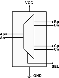
The HD3SS3411 is a high-speed bi-directional passive switch in multiplexer or demultiplexer configurations. Based on control pin SEL, the device provides switching of differential channels between Port B to Port A or Port C to Port A.
The HD3SS3411 is a generic analog differential passive switch that can work for any high speed interface application as long as it is biased at a common mode voltage range of 0 V to 2 V and has differential signaling with differential amplitude up to 1800 mVpp. The device employs adaptive tracking that ensures the channel remains unchanged for entire common mode voltage range.
Excellent dynamic characteristics of the device allow high speed switching with minimum attenuation to the signal eye diagram with little added jitter. It consumes < 2 mW of power when operational and has a shutdown mode exercisable by OEn pin resulting
< 2 µW.
Device Information(1)
| PART NUMBER | PACKAGE | BODY SIZE (NOM) |
|---|---|---|
| HD3SS3411 | WQFN (14) | 3.50 mm x 3.50 mm |
| HD3SS3411I |
- For all available packages, see the orderable addendum at the end of the data sheet.
Simplified Schematic
