SBOS508A December 2009 – December 2015 INA129-EP
PRODUCTION DATA.
- 1 Features
- 2 Applications
- 3 Description
- 4 Revision History
- 5 Pin Configuration and Functions
- 6 Specifications
- 7 Detailed Description
- 8 Application and Implementation
- 9 Power Supply Recommendations
- 10Layout
- 11Device and Documentation Support
- 12Mechanical, Packaging, and Orderable Information
Package Options
Mechanical Data (Package|Pins)
- D|8
Thermal pad, mechanical data (Package|Pins)
Orderable Information
10 Layout
10.1 Layout Guidelines
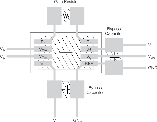
Place the power-supply bypass capacitor as closely as possible to the supply and ground pins. The recommended value of this bypass capacitor is 0.1 μF to 1 μF. If necessary, additional decoupling capacitance can be added to compensate for noisy or high-impedance power supplies. These decoupling capacitors must be placed between the power supply and INA129-EP device.
The gain resistor must be placed close to pin 1 and pin 8. This placement limits the layout loop and minimizes any noise coupling into the part.
10.2 Layout Example
 Figure 28. Recommended Layout