SBOS859B March 2018 – July 2018 INA1620
PRODUCTION DATA.
- 1 Features
- 2 Applications
- 3 Description
- 4 Revision History
- 5 Pin Configuration and Functions
- 6 Specifications
- 7 Detailed Description
- 8 Application and Implementation
- 9 Power Supply Recommendations
- 10Layout
- 11Device and Documentation Support
- 12Mechanical, Packaging, and Orderable Information
Package Options
Mechanical Data (Package|Pins)
- RTW|24
Thermal pad, mechanical data (Package|Pins)
- RTW|24
Orderable Information
7.4.1 Shutdown Mode
When the EN pin voltage is below the logic low threshold, the INA1620 enters a shutdown mode with minimal power consumption. In this state the output transistors of the amplifier are not powered on. However, do not consider the amplifier output to be high-impedance. Applying signals to the output of the INA1620 while the device is in the shutdown mode can parasitically power the output stage, causing the INA1620 output to draw current.
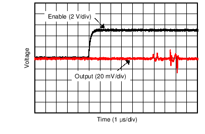
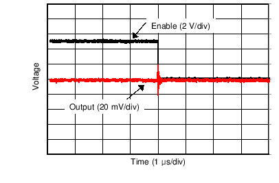
The INA1620 enable circuitry limits transients at the output when transitioning into or out of shutdown mode. However, small output transients do still accompany this transition, as illustrated in Figure 48 and Figure 49. Note that in both figures the time scale is 1 µs per division, indicating that the output transients are extremely brief in nature, and therefore not likely to be audible in headphone applications.
 Figure 48. INA1620 Output Voltage When EN Pin Transitions High (32-Ω Load Connected)
  Figure 49. INA1620 Output Voltage When EN Pin Transitions Low (32-Ω Load Connected)