SBOS818B December 2016 – November 2018 INA1650 , INA1651
PRODUCTION DATA.
- 1 Features
- 2 Applications
- 3 Description
- 4 Revision History
- 5 Pin Configuration and Functions
- 6 Specifications
- 7 Detailed Description
-
8 Application and Implementation
- 8.1 Application Information
- 8.2
Typical Applications
- 8.2.1 Line Receiver for Differential Audio Signals in a Split-Supply System
- 8.2.2 Differential Line Receiver for Single-Supply Applications
- 8.2.3 Floating Single-Ended Input Line Receiver for Ground Loop Noise Reduction
- 8.2.4 Floating Single-Ended Input Line Receiver With Differential Outputs
- 8.2.5 TRS Audio Interface in Single-Supply Applications
- 8.2.6 Differential Line Driver With Single-Ended Input
- 9 Power Supply Recommendations
- 10Layout
- 11Device and Documentation Support
- 12Mechanical, Packaging, and Orderable Information
Package Options
Mechanical Data (Package|Pins)
- PW|14
Thermal pad, mechanical data (Package|Pins)
- PW|14
Orderable Information
8.2.1.3 Application Curves
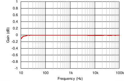
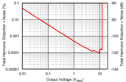
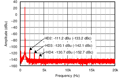
Figure 52 through Figure 57 illustrate the measured performance of the line receiver circuit. Figure 52 shows the measured frequency response. The gain of the circuit is 0 dB as expected with 0.1-dB magnitude variation at 10 Hz. The measured CMRR of the circuit (Figure 53) at 1 kHz equals 94 dB without any source impedance mismatch. Adding a 10-Ω source impedance mismatch degrades the CMRR at 1 kHz to 92 dB. The high-frequency degradation of CMRR shown in Figure 53 for the 10-Ω source impedance mismatch cases is due to the capacitance of the cables used for the measurement. The total harmonic distortion plus noise (THD+N) is plotted over frequency in Figure 54. For a 4-dBu (1.23 VRMS) input signal level, the THD+N remains flat at –101.6 dB (0.0008%) over the measured frequency range. Increasing the signal level to 22 dBu further decreases the THD+N to –115.2 dB (0.00017%) at 1 kHz, but the THD+N rises above 7 kHz. Measuring the THD+N vs Output Amplitude (Figure 55) at 1 kHz shows a constant downward slope until the noise floor of the audio analyzer is reached at 5 VRMS. The constant downward slope indicates that noise from the device dominates THD+N at this frequency instead of distortion harmonics. Figure 56 and Figure 57 confirm this conclusion. For a 4–dBu signal level, the second harmonic is barely visible above the noise floor at –140 dBu. Increasing the signal level to 22 dBu produces distortion harmonics above the noise floor. The largest harmonic in this case is the second at
–111.2 dBu, or –133.2 dB relative to the fundamental.
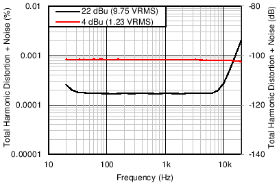
| 90-kHz Measurement Bandwidth |
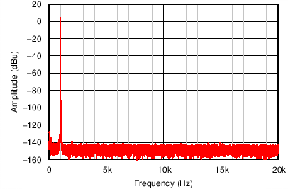
| 4–dBu Output Amplitude |
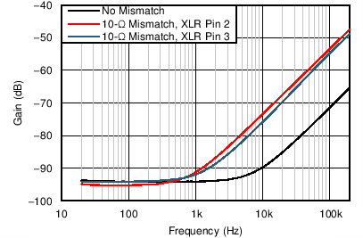
| 1-VRMS Common-Mode Signal |
| 22-kHz Measurement Bandwidth |
| 22–dBu Output Amplitude |