SBOS818B December 2016 – November 2018 INA1650 , INA1651
PRODUCTION DATA.
- 1 Features
- 2 Applications
- 3 Description
- 4 Revision History
- 5 Pin Configuration and Functions
- 6 Specifications
- 7 Detailed Description
-
8 Application and Implementation
- 8.1 Application Information
- 8.2
Typical Applications
- 8.2.1 Line Receiver for Differential Audio Signals in a Split-Supply System
- 8.2.2 Differential Line Receiver for Single-Supply Applications
- 8.2.3 Floating Single-Ended Input Line Receiver for Ground Loop Noise Reduction
- 8.2.4 Floating Single-Ended Input Line Receiver With Differential Outputs
- 8.2.5 TRS Audio Interface in Single-Supply Applications
- 8.2.6 Differential Line Driver With Single-Ended Input
- 9 Power Supply Recommendations
- 10Layout
- 11Device and Documentation Support
- 12Mechanical, Packaging, and Orderable Information
Package Options
Mechanical Data (Package|Pins)
- PW|14
Thermal pad, mechanical data (Package|Pins)
- PW|14
Orderable Information
8.1.5 Supply Divider Capacitive Loading
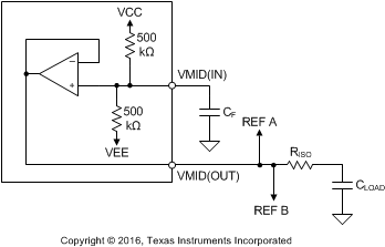
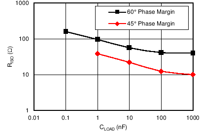
The VMID(OUT) pin of the INA165x is stable with capacitive loads up to 150 pF. An isolation resistor (RISO in Figure 49), must be used if capacitive loads larger than 150 pF are connected to the VMID(OUT) pin. Figure 49 shows the recommended configuration of an isolation resistor in series with the capacitive load. The REF pins of the INA1650 must connect directly to the VMID(OUT) pin before the isolation resistor. Any resistance placed between the VMID(OUT) pin and the reference pins degrades the CMRR of the device. Figure 50 shows the recommended value for the isolation resistor for increasing capacitive loads.
 Figure 49. Place an Isolation Resistor Between the VMID(OUT) Pin and Large Capacitive Loads
  Figure 50. Recommended Isolation Resistor Value vs Capacitive Load