SBOS576B May 2012 – March 2016 INA3221
PRODUCTION DATA.
- 1 Features
- 2 Applications
- 3 Description
- 4 Revision History
- 5 Device Comparison Table
- 6 Pin Configuration and Functions
- 7 Specifications
-
8 Detailed Description
- 8.1 Overview
- 8.2 Functional Block Diagram
- 8.3 Feature Description
- 8.4 Device Functional Modes
- 8.5 Programming
- 8.6
Register Maps
- 8.6.1 Summary of Register Set
- 8.6.2
Register Descriptions
- 8.6.2.1 Configuration Register (address = 00h) [reset = 7127h]
- 8.6.2.2 Channel-1 Shunt-Voltage Register (address = 01h), [reset = 00h]
- 8.6.2.3 Channel-1 Bus-Voltage Register (address = 02h) [reset = 00h]
- 8.6.2.4 Channel-2 Shunt-Voltage Register (address = 03h) [reset = 00h]
- 8.6.2.5 Channel-2 Bus-Voltage Register (address = 04h) [reset = 00h]
- 8.6.2.6 Channel-3 Shunt-Voltage Register (address = 05h) [reset = 00h]
- 8.6.2.7 Channel-3 Bus-Voltage Register (address = 06h) [reset = 00h]
- 8.6.2.8 Channel-1 Critical-Alert Limit Register (address = 07h) [reset = 7FF8h]
- 8.6.2.9 Warning-Alert Channel-1 Limit Register (address = 08h) [reset = 7FF8h]
- 8.6.2.10 Channel-2 Critical-Alert Limit Register (address = 09h) [reset = 7FF8h]
- 8.6.2.11 Channel-2 Warning-Alert Limit Register (address = 0Ah) [reset = 7FF8h]
- 8.6.2.12 Channel-3 Critical-Alert Limit Register (address = 0Bh) [reset = 7FF8h]
- 8.6.2.13 Channel-3 Warning-Alert Limit Register (address = 0Ch) [reset = 7FF8h]
- 8.6.2.14 Shunt-Voltage Sum Register (address = 0Dh) [reset = 00h]
- 8.6.2.15 Shunt-Voltage Sum-Limit Register (address = 0Eh) [reset = 7FFEh]
- 8.6.2.16 Mask/Enable Register (address = 0Fh) [reset = 0002h]
- 8.6.2.17 Power-Valid Upper-Limit Register (address = 10h) [reset = 2710h]
- 8.6.2.18 Power-Valid Lower-Limit Register (address = 11h) [reset = 2328h]
- 8.6.2.19 Manufacturer ID Register (address = FEh) [reset = 5449h]
- 8.6.2.20 Die ID Register (address = FFh) [reset = 3220]
- 9 Application and Implementation
- 10Power Supply Recommendations
- 11Layout
- 12Device and Documentation Support
- 13Mechanical, Packaging, and Orderable Information
Package Options
Mechanical Data (Package|Pins)
- RGV|16
Thermal pad, mechanical data (Package|Pins)
- RGV|16
Orderable Information
1 Features
2 Applications
- Computers
- Power Management
- Telecom Equipment
- Battery Chargers
- Power Supplies
- Test Equipment
3 Description
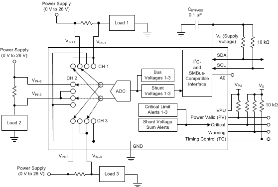
The INA3221 is a three-channel, high-side current and bus voltage monitor with an I2C- and SMBUS-compatible interface. The INA3221 monitors both shunt voltage drops and bus supply voltages, in addition to having programmable conversion times and averaging modes for these signals. The INA3221 offers both critical and warning alerts to detect multiple programmable out-of-range conditions for each channel.
The INA3221 senses current on buses that can vary from 0 V to 26 V. The device is powered from a single 2.7-V to 5.5-V supply, and draws 350 μA (typ) of supply current. The INA3221 is specified over the operating temperature range of –40°C to +125°C. The I2C- and SMBUS-compatible interface features four programmable addresses.
Device Information(1)
| PART NUMBER | PACKAGE | BODY SIZE (NOM) |
|---|---|---|
| INA3221 | VQFN (16) | 4.00 mm x 4.00 mm |
- For all available packages, see the package option addendum at the end of the datasheet.
