SBOS576B May 2012 – March 2016 INA3221
PRODUCTION DATA.
- 1 Features
- 2 Applications
- 3 Description
- 4 Revision History
- 5 Device Comparison Table
- 6 Pin Configuration and Functions
- 7 Specifications
-
8 Detailed Description
- 8.1 Overview
- 8.2 Functional Block Diagram
- 8.3 Feature Description
- 8.4 Device Functional Modes
- 8.5 Programming
- 8.6
Register Maps
- 8.6.1 Summary of Register Set
- 8.6.2
Register Descriptions
- 8.6.2.1 Configuration Register (address = 00h) [reset = 7127h]
- 8.6.2.2 Channel-1 Shunt-Voltage Register (address = 01h), [reset = 00h]
- 8.6.2.3 Channel-1 Bus-Voltage Register (address = 02h) [reset = 00h]
- 8.6.2.4 Channel-2 Shunt-Voltage Register (address = 03h) [reset = 00h]
- 8.6.2.5 Channel-2 Bus-Voltage Register (address = 04h) [reset = 00h]
- 8.6.2.6 Channel-3 Shunt-Voltage Register (address = 05h) [reset = 00h]
- 8.6.2.7 Channel-3 Bus-Voltage Register (address = 06h) [reset = 00h]
- 8.6.2.8 Channel-1 Critical-Alert Limit Register (address = 07h) [reset = 7FF8h]
- 8.6.2.9 Warning-Alert Channel-1 Limit Register (address = 08h) [reset = 7FF8h]
- 8.6.2.10 Channel-2 Critical-Alert Limit Register (address = 09h) [reset = 7FF8h]
- 8.6.2.11 Channel-2 Warning-Alert Limit Register (address = 0Ah) [reset = 7FF8h]
- 8.6.2.12 Channel-3 Critical-Alert Limit Register (address = 0Bh) [reset = 7FF8h]
- 8.6.2.13 Channel-3 Warning-Alert Limit Register (address = 0Ch) [reset = 7FF8h]
- 8.6.2.14 Shunt-Voltage Sum Register (address = 0Dh) [reset = 00h]
- 8.6.2.15 Shunt-Voltage Sum-Limit Register (address = 0Eh) [reset = 7FFEh]
- 8.6.2.16 Mask/Enable Register (address = 0Fh) [reset = 0002h]
- 8.6.2.17 Power-Valid Upper-Limit Register (address = 10h) [reset = 2710h]
- 8.6.2.18 Power-Valid Lower-Limit Register (address = 11h) [reset = 2328h]
- 8.6.2.19 Manufacturer ID Register (address = FEh) [reset = 5449h]
- 8.6.2.20 Die ID Register (address = FFh) [reset = 3220]
- 9 Application and Implementation
- 10Power Supply Recommendations
- 11Layout
- 12Device and Documentation Support
- 13Mechanical, Packaging, and Orderable Information
Package Options
Mechanical Data (Package|Pins)
- RGV|16
Thermal pad, mechanical data (Package|Pins)
- RGV|16
Orderable Information
9 Application and Implementation
NOTE
Information in the following applications sections is not part of the TI component specification, and TI does not warrant its accuracy or completeness. TI’s customers are responsible for determining suitability of components for their purposes. Customers should validate and test their design implementation to confirm system functionality.
9.1 Application Information
INA3221 is a three-channel current and bus voltage monitor with I2C/SMBUS-compatible interface. It features programmable conversion times and averaging modes and offers both critical and warning alerts to detect multiple programmable out-of-range conditions for each channel.
9.2 Typical Application
The INA3221 measures the voltage developed across a current-sensing resistor when current passes through it. The device also measures the bus supply voltage at the IN- pin. Multiple monitoring functions are supported using four alert pins: Critical, Warning, PV, and TC. Programmable thresholds make sure operation is within desired operating conditions. This design illustrates the ability of the Critical alert pin to respond to a set threshold.
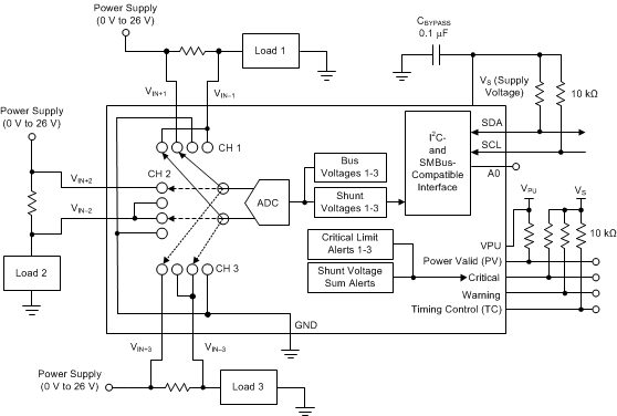
Figure 32 illustrates a typical INA3221 application circuit using all three channels. For best performance, use a 0.1-μF ceramic capacitor for power-supply bypassing, placed as close as possible to the supply and ground pins. The digital pins (SCL, SDA, Critical, Warning, TC) are connected to supply through pull-up resistors. The power valid (PV) alert pin is connected to the VPU pin through a pull-up resistor to enable power-valid monitoring.
9.2.1 Design Requirements
For this design example, use the input parameters shown in Table 45. All other register settings are default.
Table 45. Design Parameters
| DESIGN PARAMETER | EXAMPLE VALUE |
|---|---|
| Supply voltage, VS | 5 V |
| Pull-up resistors | 10 kΩ |
| Input range | –163.84 to +163.8 |
| Enabled channel | CH1 |
| Operating mode | Shunt voltage, continuous |
| Average setting | 1 |
| Critical alert limit | 80 mV |
| Critical Alert Limit register setting | 7D0h |
9.2.2 Detailed Design Procedure
This design shows two shunt voltage conversion times in order to demonstrate the difference in the alert response times. This design generates a critical-alert response when the input voltage exceeds 80 mV on channel 1. See Table 45 for all design parameters.
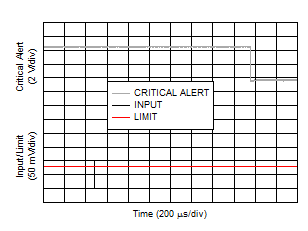
For the first example the shunt voltage conversion time is set to 1.1 ms. When the input signal exceeds 80 mV, the Critical alert pin pulls low after the conversion cycle completes, indicating an overcurrent condition, as shown in Figure 33.
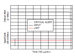
For the second example, the conversion time is set to 588 µs, and the response is shown in Figure 34.
9.2.3 Application Curves
Figure 33 shows the Critical alert pin response to a shunt voltage overlimit of 80 mV for a conversion time of 1.1 ms. Figure 34 shows the response for the same limit, but with the conversion time reduced to 588 µs.

| Configuration register = 4125h, conversion time = 588 µs |

| Configuration register = 40DDh, conversion time = 588 µs |
