SBOS074E September   1997  – June 2018 ISO124

PRODUCTION DATA.  

  1. Features
  2. Applications
  3. Description
    1.     Device Images
      1.      Simplified Schematic
  4. Revision History
  5. Pin Configuration and Functions
    1.     Pin Functions
  6. Specifications
    1. 6.1 Absolute Maximum Ratings
    2. 6.2 ESD Ratings
    3. 6.3 Recommended Operating Conditions
    4. 6.4 Thermal Information
    5. 6.5 Electrical Characteristics
    6. 6.6 Typical Characteristics
  7. Detailed Description
    1. 7.1 Overview
      1. 7.1.1 Modulator
      2. 7.1.2 Demodulator
    2. 7.2 Functional Block Diagram
    3. 7.3 Feature Description
      1. 7.3.1 Isolation Amplifier
    4. 7.4 Device Functional Modes
  8. Application and Implementation
    1. 8.1 Application Information
      1. 8.1.1 Carrier Frequency Considerations
      2. 8.1.2 Isolation Mode Voltage Induced Errors
      3. 8.1.3 High IMV dV/dt Errors
      4. 8.1.4 High Voltage Testing
    2. 8.2 Typical Applications
      1. 8.2.1 Output Filters
        1. 8.2.1.1 Design Requirements
        2. 8.2.1.2 Detailed Design Procedure
        3. 8.2.1.3 Application Curves
      2. 8.2.2 Battery Monitor
      3. 8.2.3 Programmable Gain Amplifier
      4. 8.2.4 Thermocouple Amplifier
      5. 8.2.5 Isolated 4-mA to 20-mA Instrument Loop
      6. 8.2.6 Single-Supply Operation of the ISO124 Isolation Amplifier
      7. 8.2.7 Input-Side Powered ISO Amplifier
      8. 8.2.8 Powered ISO Amplifier With Three-Port Isolation
  9. Power Supply Recommendations
    1. 9.1 Signal and Supply Connections
  10. 10Layout
    1. 10.1 Layout Guidelines
    2. 10.2 Layout Example
  11. 11Device and Documentation Support
    1. 11.1 Documentation Support
      1. 11.1.1 Related Documentation
    2. 11.2 Receiving Notification of Documentation Updates
    3. 11.3 Community Resources
    4. 11.4 Trademarks
    5. 11.5 Electrostatic Discharge Caution
    6. 11.6 Glossary
  12. 12Mechanical, Packaging, and Orderable Information

Package Options

Refer to the PDF data sheet for device specific package drawings

Mechanical Data (Package|Pins)
  • NVF|8
  • DVA|8
Thermal pad, mechanical data (Package|Pins)
Orderable Information

Typical Characteristics

at TA = +25°C, and VS = ±15 V (unless otherwise noted)
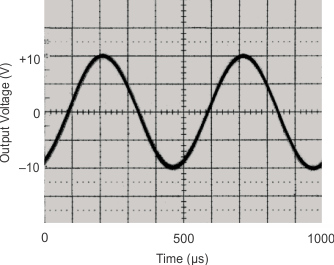
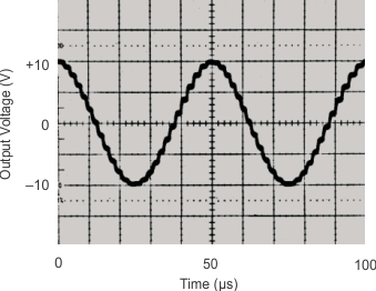
ISO124 graph_1_sbos074.gif
f = 2 kHz
Figure 1. Sine Response
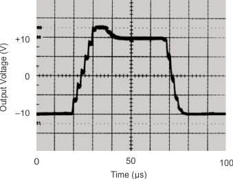
ISO124 graph_3_sbos074.gif
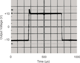
Figure 3. Step Response
ISO124 graph_5_sbos074.gif
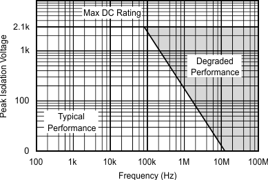
Figure 5. Isolation Voltage vs Frequency
ISO124 graph_7_sbos074.gif
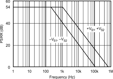
Figure 7. PSRR vs Frequency
ISO124 graph_9_sbos074.gif
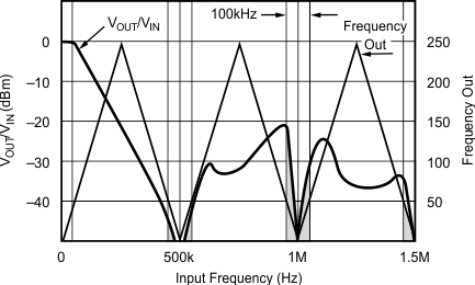
NOTE: Shaded area shows aliasing frequencies that cannot be removed by a low-pass filter at the output.
Figure 9. Signal Response to Inputs Greater than 250 kHz
ISO124 graph_2_sbos074.gif
f = 20 kHz
Figure 2. Sine Response
ISO124 graph_4_sbos074.gif
Figure 4. Step Response
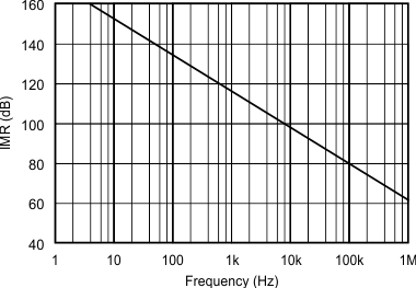
ISO124 graph_6_sbos074.gif
Figure 6. IMR vs Frequency
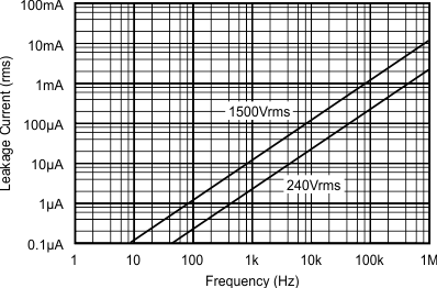
ISO124 graph_8_sbos074.gif
Figure 8. Isolation Leakage Current vs Frequency