SLLS867K September 2007 – October 2015 ISO7230C , ISO7230M , ISO7231C , ISO7231M
PRODUCTION DATA.
- 1 Features
- 2 Applications
- 3 Description
- 4 Revision History
- 5 Device Comparison Table
- 6 Pin Configuration and Functions
-
7 Specifications
- 7.1 Absolute Maximum Ratings
- 7.2 ESD Ratings
- 7.3 Recommended Operating Conditions
- 7.4 Thermal Information
- 7.5 Electrical Characteristics: VCC1 and VCC2 at 5-V
- 7.6 Electrical Characteristics: VCC1 at 5-V, VCC2 at 3.3-V
- 7.7 Electrical Characteristics: VCC1 at 3.3-V, VCC2 at 5-V
- 7.8 Electrical Characteristics: VCC1 and VCC2 at 3.3 V
- 7.9 Power Dissipation Characteristics
- 7.10 Switching Characteristics: VCC1 and VCC2 at 5-V
- 7.11 Switching Characteristics: VCC1 at 5-V, VCC2 at 3.3-V
- 7.12 Switching Characteristics: VCC1 at 3.3-V and VCC2 at 5-V
- 7.13 Switching Characteristics: VCC1 and VCC2 at 3.3-V
- 7.14 Typical Characteristics
- 8 Parameter Measurement Information
- 9 Detailed Description
- 10Application and Implementation
- 11Power Supply Recommendations
- 12Layout
- 13Device and Documentation Support
- 14Mechanical, Packaging, and Orderable Information
Package Options
Refer to the PDF data sheet for device specific package drawings
Mechanical Data (Package|Pins)
- DW|16
Thermal pad, mechanical data (Package|Pins)
Orderable Information
1 Features
- 25 and 150-Mbps Signaling Rate Options
- Low Channel-to-Channel Output Skew;
1 ns Maximum - Low Pulse-Width Distortion (PWD);
2 ns Maximum - Low Jitter Content; 1 ns Typical at 150 Mbps
- Low Channel-to-Channel Output Skew;
- Typical 25-Year Life at Rated Working Voltage
(See Application Note SLLA197 and Figure 19) - 4-kV ESD Protection
- Operate With 3.3-V or 5-V Supplies
- 3.3-V and 5-V Level Translation
- High Electromagnetic Immunity
(See Application Note SLLA181) - –40°C to 125°C Operating Range
- Safety and Regulatory Approvals
- 4000-VPK Isolation per DIN V VDE V 0884-10 and DIN EN 61010-1
- 2500 VRMS Isolation for 1 minute per UL 1577
- CSA Component Acceptance Notice 5A and IEC 60950-1 End Equipment Standard
2 Applications
- Industrial Fieldbus
- Computer Peripheral Interface
- Servo Control Interface
- Data Acquisition
3 Description
The ISO7230 and ISO7231 are triple-channel digital isolators each with multiple channel configurations and output enable functions. These devices have logic input and output buffers separated by TI’s silicon dioxide (SiO2) isolation barrier. Used in conjunction with isolated power supplies, these devices block high voltage, isolate grounds, and prevent noise currents on a data bus or other circuits from entering the local ground and interfering with or damaging sensitive circuitry.
Device Information(1)
| PART NUMBER | PACKAGE | BODY SIZE (NOM) |
|---|---|---|
| ISO7230C ISO7230M ISO7231C ISO7231M |
SOIC (16) | 10.30 mm × 7.50 mm |
- For all available packages, see the orderable addendum at the end of the datasheet.
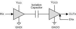
Simplified Schematic

1. VCCI and GNDI are supply and ground connections respectively for the input channels.
2. VCCO and GNDO are supply and ground connections respectively for the output channels.