SLLS868T September 2007 – April 2017 ISO7240C , ISO7240CF , ISO7240M , ISO7241C , ISO7241M , ISO7242C , ISO7242M
PRODUCTION DATA.
- 1 Features
- 2 Applications
- 3 Description
- 4 Revision History
- 5 Description (Continued)
- 6 Pin Configurations and Functions
-
7 Specifications
- 7.1 Absolute Maximum Ratings
- 7.2 ESD Ratings
- 7.3 Recommended Operating Conditions
- 7.4 Thermal Information
- 7.5 Power Ratings
- 7.6 Insulation Specifications
- 7.7 Safety-Related Certifications
- 7.8 Safety Limiting Values
- 7.9 Electrical Characteristics: VCC1 and VCC2 at 5-V Operation
- 7.10 Supply Current Characteristics: VCC1 and VCC2 at 5-V Operation
- 7.11 Electrical Characteristics: VCC1 at 5-V, VCC2 at 3.3-V Operation
- 7.12 Supply Current Characteristics: VCC1 at 5-V, VCC2 at 3.3-V Operation
- 7.13 Electrical Characteristics: VCC1 at 3.3-V, VCC2 at 5-V Operation
- 7.14 Supply Current Characteristics: VCC1 at 3.3-V, VCC2 at 5-V Operation
- 7.15 Electrical Characteristics: VCC1 and VCC2 at 3.3 V Operation
- 7.16 Supply Current Characteristics: VCC1 and VCC2 at 3.3 V Operation
- 7.17 Switching Characteristics: VCC1 and VCC2 at 5-V Operation
- 7.18 Switching Characteristics: VCC1 at 5-V, VCC2 at 3.3-V Operation
- 7.19 Switching Characteristics: VCC1 at 3.3-V and VCC2 at 5-V Operation
- 7.20 Switching Characteristics: VCC1 and VCC2 at 3.3-V Operation
- 7.21 Insulation Characteristics Curves
- 7.22 Typical Characteristics
- 8 Parameter Measurement Information
- 9 Detailed Description
- 10Application and Implementation
- 11Power Supply Recommendations
- 12Layout
- 13Device and Documentation Support
- 14Mechanical, Packaging, and Orderable Information
Package Options
Mechanical Data (Package|Pins)
- DW|16
Thermal pad, mechanical data (Package|Pins)
Orderable Information
7 Specifications
7.1 Absolute Maximum Ratings
See (1)| MIN | MAX | UNIT | |||||
|---|---|---|---|---|---|---|---|
| VCC | Supply voltage(2), VCC1, VCC2 | –0.5 | 6 | V | |||
| VI | Voltage at IN, OUT, EN, DISABLE, CTRL | –0.5 | VCC + 0.5(3) | V | |||
| IO | Output current | –15 | 15 | mA | |||
| TJ | Maximum junction temperature | 170 | °C | ||||
| Tstg | Storage temperature | –65 | 150 | °C | |||
(1) Stresses beyond those listed under Absolute Maximum Ratings may cause permanent damage to the device. These are stress ratings only and functional operation of the device at these or any other conditions beyond those indicated under Recommended Operating Conditions is not implied. Exposure to absolute-maximum-rated conditions for extended periods may affect device reliability.
(2) All voltage values are with respect to network ground terminal and are peak voltage values.
(3) Maximum voltage must not exceed 6 V.
7.2 ESD Ratings
| VALUE | UNIT | ||||||
|---|---|---|---|---|---|---|---|
| V(ESD) | Electrostatic discharge | Human body model (HBM), per ANSI/ESDA/JEDEC JS-001(1) | ±4000 | V | |||
| Charged device model (CDM), per JEDEC specification JESD22-C101(2) | ±1000 | ||||||
| Machine model (MM), per ANSI/ESDS5.2-1996 | ±200 | ||||||
(1) JEDEC document JEP155 states that 500-V HBM allows safe manufacturing with a standard ESD control process.
(2) JEDEC document JEP157 states that 250-V CDM allows safe manufacturing with a standard ESD control process.
7.3 Recommended Operating Conditions
| MIN | NOM | MAX | UNIT | |||
|---|---|---|---|---|---|---|
| VCC | Supply voltage(2), VCC1, VCC2 | 3.15 | 5.5 | V | ||
| IOH | High-level output current | –4 | mA | |||
| IOL | Low-level output current | 4 | mA | |||
| tui | Input pulse width | ISO724xC | 40 | ns | ||
| ISO724xM | 6.67 | 5 | ||||
| 1/tui | Signaling rate | ISO724xC | 0 | 30(1) | 25 | Mbps |
| ISO724xM | 0 | 200(1) | 150 | |||
| VIH | High-level input voltage (IN) | ISO724xM | 0.7 VCC | VCC | V | |
| VIL | Low-level input voltage (IN) | 0 | 0.3 VCC | V | ||
| VIH | High-level input voltage (IN, DISABLE, CTRL, EN) | ISO724xC | 2 | 5.5 | V | |
| VIL | Low-level input voltage (IN, DISABLE, CTRL, EN) | 0 | 0.8 | V | ||
| TJ | Junction temperature | 150 | °C | |||
| H | External magnetic field-strength immunity per IEC 61000-4-8 and IEC 61000-4-9 certification | 1000 | A/m | |||
(1) Typical value at room temperature and well-regulated power supply.
(2) For the 5-V operation, VCC1 or VCC2 is specified from 4.5 V to 5.5 V.
For the 3.3-V operation, VCC1 or VCC2 is specified from 3.15 V to 3.6 V.
For the 3.3-V operation, VCC1 or VCC2 is specified from 3.15 V to 3.6 V.
7.4 Thermal Information
| THERMAL METRIC(1) | ISO724xx | UNIT | ||
|---|---|---|---|---|
| DW (SOIC) | ||||
| 16 PINS | ||||
| RθJA | Junction-to-ambient thermal resistance | Low-K board | 168 | °C/W |
| High-K board | 77.3 | °C/W | ||
| RθJC(top) | Junction-to-case (top) thermal resistance | 39.5 | °C/W | |
| RθJB | Junction-to-board thermal resistance | 41.9 | °C/W | |
| ψJT | Junction-to-top characterization parameter | 13.5 | °C/W | |
| ψJB | Junction-to-board characterization parameter | 41.9 | °C/W | |
| RθJC(bot) | Junction-to-case (bottom) thermal resistance | n/a | °C/W | |
(1) For more information about traditional and new thermal metrics, see the Semiconductor and IC Package Thermal Metrics application report.
7.5 Power Ratings
VCC1 = VCC2 = 5.5 V, TJ = 150°C, CL = 15 pF, Input a 50% duty cycle square wave (unless otherwise noted)| PARAMETER | TEST CONDITIONS | MIN | TYP | MAX | UNIT | |
|---|---|---|---|---|---|---|
| PD | Maximum power dissipation | 220 | mW | |||
7.6 Insulation Specifications
| PARAMETER | TEST CONDITIONS | VALUE | UNIT | |
|---|---|---|---|---|
| GENERAL | ||||
| CLR | External clearance(1) | Shortest terminal-to-terminal distance through air | 8 | mm |
| CPG | External creepage(1) | Shortest terminal-to-terminal distance across the package surface | 8 | mm |
| DTI | Distance through the insulation | Minimum internal gap (internal clearance) | 0.008 | mm |
| CTI | Comparative tracking index | DIN EN 60112 (VDE 0303-11); IEC 60112 | ≥ 400 | V |
| Material group | II | |||
| Overvoltage Category | Rated mains voltage ≤ 150 VRMS | I-IV | ||
| Rated mains voltage ≤ 300 VRMS | I-III | |||
| DIN V VDE V 0884-10 (VDE V 0884-10):2006-12(2) | ||||
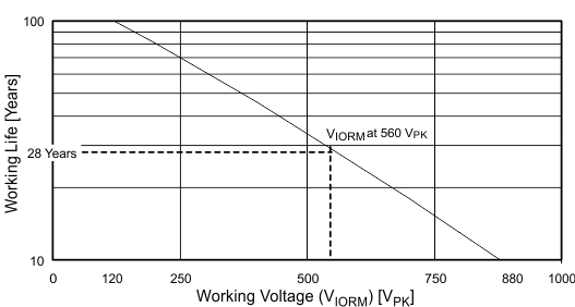
| VIORM | Maximum repetitive peak isolation voltage | AC voltage (bipolar) | 560 | VPK |
| VIOTM | Maximum transient isolation voltage | VTEST = VIOTM
t = 60 s (qualification), t = 1 s (100% production) |
4000 | VPK |
| qpd | Apparent charge(3) | Method a: After I/O safety test subgroup 2/3. Vini = VIOTM, tini = 60 s; Vpd(m) = 1.2 × VIORM , tm = 10 s, |
≤5 | pC |
| Method a: After environmental tests subgroup 1, Vini = VIOTM, tini = 60 s; Vpd(m) = 1.3 × VIORM , tm = 10 s, |
≤5 | |||
| Method b1: At routine test (100% production) and preconditioning (type test) Vini = VIOTM, tini = 1 s; Vpd(m) = 1.5 × VIORM , tm = 1 s, |
≤5 | |||
| CIO | Barrier capacitance, input to output(4) | VI = 0.4 sin (4E6πt) | 2 | pF |
| RIO | Isolation resistance, input to output(4) | VIO = 500 V, TA = 25°C | > 1012 | Ω |
| VIO = 500 V, 100°C ≤ TA ≤ 125°C | >1011 | |||
| VIO = 500 V at TS = 150°C | >109 | |||
| Pollution degree | 2 | |||
| Climatic category | 40/125/21 | |||
| UL 1577 | ||||
| VISO | Withstand isolation voltage | VTEST = VISO = 2500 VRMS, t = 60 s (qualification); VTEST = 1.2 × VISO = 3000 VRMS, t = 1 s (100% production) | 2500 | VRMS |
(1) Creepage and clearance requirements should be applied according to the specific equipment isolation standards of an application. Care should be taken to maintain the creepage and clearance distance of a board design to ensure that the mounting pads of the isolator on the printed-circuit board do not reduce this distance. Creepage and clearance on a printed-circuit board become equal in certain cases. Techniques such as inserting grooves and/or ribs on a printed circuit board are used to help increase these specifications.
(2) This coupler is suitable for basic electrical insulation only within the maximum operating ratings. Compliance with the safety ratings shall be ensured by means of suitable protective circuits.
(3) Apparent charge is electrical discharge caused by a partial discharge (pd).
(4) All pins on each side of the barrier tied together creating a two-terminal device
7.7 Safety-Related Certifications
7.8 Safety Limiting Values
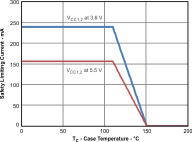
Safety limiting(1) intends to minimize potential damage to the isolation barrier upon failure of input or output circuitry. A failure of the I/O can allow low resistance to ground or the supply and, without current limiting, dissipate sufficient power to overheat the die and damage the isolation barrier, potentially leading to secondary system failures.| PARAMETER | TEST CONDITIONS | MIN | TYP | MAX | UNIT | |
|---|---|---|---|---|---|---|
| IS | Safety input, output, or supply current | RθJA = 168°C/W, VI = 5.5 V, TJ = 170°C, TA = 25°C, see Figure 2 | 156 | mA | ||
| RθJA = 168°C/W, VI = 3.6 V, TJ = 170°C, TA = 25°C, see Figure 2 | 239 | |||||
| TS | Safety temperature | 150 | °C | |||
(1) The safety-limiting constraint is the maximum junction temperature specified in the data sheet. The power dissipation and junction-to-air thermal impedance of the device installed in the application hardware determines the junction temperature. The assumed junction-to-air thermal resistance in the Thermal Information table is that of a device installed on a high-K test board for leaded surface-mount packages. The power is the recommended maximum input voltage times the current. The junction temperature is then the ambient temperature plus the power times the junction-to-air thermal resistance.
7.9 Electrical Characteristics: VCC1 and VCC2 at 5-V Operation
For the 5-V operation, VCC1 or VCC2 is specified from 4.5 V to 5.5 V. Over recommended operating conditions (unless otherwise noted)| PARAMETER | TEST CONDITIONS | MIN | TYP | MAX | UNIT | |
|---|---|---|---|---|---|---|
| IOFF | Sleep mode output current | EN at 0 V, Single channel | 0 | μA | ||
| VOH | High-level output voltage | IOH = –4 mA, See Figure 11 | VCCO – 0.8 | V | ||
| IOH = –20 μA, See Figure 11 | VCCO – 0.1 | |||||
| VOL | Low-level output voltage | IOL = 4 mA, See Figure 11 | 0.4 | V | ||
| IOL = 20 μA, See Figure 11 | 0.1 | |||||
| VI(HYS) | Input voltage hysteresis | 150 | mV | |||
| IIH | High-level input current | IN at VCCI | 10 | μA | ||
| IIL | Low-level input current | IN at 0 V | –10 | |||
| CI | Input capacitance to ground | IN at VCC, VI = 0.4 sin (4E6πt) | 2 | pF | ||
| CMTI | Common-mode transient immunity | VI = VCC or 0 V, See Figure 15 | 25 | 50 | kV/μs | |
7.10 Supply Current Characteristics: VCC1 and VCC2 at 5-V Operation
For the 5-V operation, VCC1 or VCC2 is specified from 4.5 V to 5.5 V. Over recommended operating conditions (unless otherwise noted)7.11 Electrical Characteristics: VCC1 at 5-V, VCC2 at 3.3-V Operation
For the 5-V operation, VCC1 or VCC2 is specified from 4.5 V to 5.5 V. For the 3.3-V operation, VCC1 or VCC2 is specified from 3.15 V to 3.6 V. Over recommended operating conditions (unless otherwise noted)| PARAMETER | TEST CONDITIONS | MIN | TYP | MAX | UNIT | ||
|---|---|---|---|---|---|---|---|
| IOFF | Sleep mode output current | EN at 0 V, Single channel | 0 | μA | |||
| VOH | High-level output voltage | IOH = –4 mA, See Figure 11 | 3.3-V side | VCCO – 0.4 | V | ||
| 5-V side | VCCO – 0.8 | ||||||
| IOH = –20 μA, See Figure 11 | VCCO – 0.1 | ||||||
| VOL | Low-level output voltage | IOL = 4 mA, See Figure 11 | 0.4 | V | |||
| IOL = 20 μA, See Figure 11 | 0.1 | ||||||
| VI(HYS) | Input voltage hysteresis | 150 | mV | ||||
| IIH | High-level input current | IN at VCCI | 10 | μA | |||
| IIL | Low-level input current | IN at 0 V | –10 | ||||
| CI | Input capacitance to ground | IN at VCC, VI = 0.4 sin (4E6πt) | 2 | pF | |||
| CMTI | Common-mode transient immunity | VI = VCC or 0 V, See Figure 15 | 25 | 50 | kV/μs | ||
7.12 Supply Current Characteristics: VCC1 at 5-V, VCC2 at 3.3-V Operation
For the 5-V operation, VCC1 or VCC2 is specified from 4.5 V to 5.5 V. For the 3.3-V operation, VCC1 or VCC2 is specified from 3.15 V to 3.6 V. Over recommended operating conditions (unless otherwise noted)7.13 Electrical Characteristics: VCC1 at 3.3-V, VCC2 at 5-V Operation
For the 5-V operation, VCC1 or VCC2 is specified from 4.5 V to 5.5 V. For the 3.3-V operation, VCC1 or VCC2 is specified from 3.15 V to 3.6 V. Over recommended operating conditions (unless otherwise noted)| PARAMETER | TEST CONDITIONS | MIN | TYP | MAX | UNIT | ||
|---|---|---|---|---|---|---|---|
| IOFF | Sleep mode output current | EN at 0 V, Single channel | 0 | μA | |||
| VOH | High-level output voltage | IOH = –4 mA, See Figure 11 | 3.3-V side | VCCO – 0.4 | V | ||
| 5-V side | VCCO – 0.8 | ||||||
| IOH = –20 μA, See Figure 11 | VCCO – 0.1 | ||||||
| VOL | Low-level output voltage | IOL = 4 mA, See Figure 11 | 0.4 | V | |||
| IOL = 20 μA, See Figure 11 | 0.1 | ||||||
| VI(HYS) | Input voltage hysteresis | 150 | mV | ||||
| IIH | High-level input current | IN at VCCI | 10 | μA | |||
| IIL | Low-level input current | IN at 0 V | –10 | ||||
| CI | Input capacitance to ground | IN at VCC, VI = 0.4 sin (4E6πt) | 2 | pF | |||
| CMTI | Common-mode transient immunity | VI = VCC or 0 V, See Figure 15 | 25 | 50 | kV/μs | ||
7.14 Supply Current Characteristics: VCC1 at 3.3-V, VCC2 at 5-V Operation
For the 5-V operation, VCC1 or VCC2 is specified from 4.5 V to 5.5 V. For the 3.3-V operation, VCC1 or VCC2 is specified from 3.15 V to 3.6 V. Over recommended operating conditions (unless otherwise noted)7.15 Electrical Characteristics: VCC1 and VCC2 at 3.3 V Operation
For the 3.3-V operation, VCC1 or VCC2 is specified from 3.15 V to 3.6 V. Over recommended operating conditions (unless otherwise noted)| PARAMETER | TEST CONDITIONS | MIN | TYP | MAX | UNIT | |
|---|---|---|---|---|---|---|
| IOFF | Sleep mode output current | EN at 0 V, single channel | 0 | μA | ||
| VOH | High-level output voltage | IOH = –4 mA, See Figure 11 | VCCO – 0.4 | V | ||
| IOH = –20 μA, See Figure 11 | VCCO – 0.1 | |||||
| VOL | Low-level output voltage | IOL = 4 mA, See Figure 11 | 0.4 | V | ||
| IOL = 20 μA, See Figure 11 | 0.1 | |||||
| VI(HYS) | Input voltage hysteresis | 150 | mV | |||
| IIH | High-level input current | IN at VCCI | 10 | μA | ||
| IIL | Low-level input current | IN at 0 V | –10 | |||
| CI | Input capacitance to ground | IN at VCC, VI = 0.4 sin (4E6πt) | 2 | pF | ||
| CMTI | Common-mode transient immunity | VI = VCC or 0 V, See Figure 15 | 25 | 50 | kV/μs | |
7.16 Supply Current Characteristics: VCC1 and VCC2 at 3.3 V Operation
For the 3.3-V operation, VCC1 or VCC2 is specified from 3.15 V to 3.6 V. Over recommended operating conditions (unless otherwise noted)7.17 Switching Characteristics: VCC1 and VCC2 at 5-V Operation
over recommended operating conditions (unless otherwise noted)| PARAMETER | TEST CONDITIONS | MIN | TYP | MAX | UNIT | ||
|---|---|---|---|---|---|---|---|
| tPLH, tPHL | Propagation delay | ISO724xC | See Figure 11 | 18 | 42 | ns | |
| PWD | Pulse-width distortion(1) |tPHL – tPLH| | 2.5 | |||||
| tPLH, tPHL | Propagation delay | ISO724xM | 10 | 23 | ns | ||
| PWD | Pulse-width distortion(1) |tPHL – tPLH| | 1 | 2 | ||||
| tsk(pp) | Part-to-part skew (2) | ISO724xC | 8 | ns | |||
| ISO724xM | 0 | 3 | |||||
| tsk(o) | Channel-to-channel output skew (3) | ISO724xC | 2 | ns | |||
| ISO724xM | 0 | 1 | |||||
| tr | Output signal rise time | See Figure 11 | 2 | ns | |||
| tf | Output signal fall time | 2 | |||||
| tPHZ | Propagation delay, high-level-to-high-impedance output | See Figure 12 | 15 | 20 | ns | ||
| tPZH | Propagation delay, high-impedance-to-high-level output | 15 | 20 | ||||
| tPLZ | Propagation delay, low-level-to-high-impedance output | 15 | 20 | ||||
| tPZL | Propagation delay, high-impedance-to-low-level output | 15 | 20 | ||||
| tfs | Failsafe output delay time from input power loss | See Figure 13 | 12 | μs | |||
| twake | Wake time from input disable | See Figure 14 | 15 | μs | |||
| tjit(pp) | Peak-to-peak eye-pattern jitter | ISO724xM | 150 Mbps NRZ data input, Same polarity input on all channels, See Figure 16 | 1 | ns | ||
(1) Also referred to as pulse skew.
7.18 Switching Characteristics: VCC1 at 5-V, VCC2 at 3.3-V Operation
over recommended operating conditions (unless otherwise noted)| PARAMETER | TEST CONDITIONS | MIN | TYP | MAX | UNIT | ||
|---|---|---|---|---|---|---|---|
| tPLH, tPHL | Propagation delay | ISO724xC | See Figure 11 | 20 | 50 | ns | |
| PWD | Pulse-width distortion(1) |tPHL – tPLH| | 3 | |||||
| tPLH, tPHL | Propagation delay | ISO724xM | 12 | 29 | ns | ||
| PWD | Pulse-width distortion(1) |tPHL – tPLH| | 1 | 2 | ||||
| tsk(pp) | Part-to-part skew (1) | ISO724xC | 10 | ns | |||
| ISO724xM | 0 | 5 | |||||
| tsk(o) | Channel-to-channel output skew (3) | ISO724xC | 3 | ns | |||
| ISO724xM | 0 | 1 | |||||
| tr | Output signal rise time | See Figure 11 | 2 | ns | |||
| tf | Output signal fall time | 2 | |||||
| tPHZ | Propagation delay, high-level-to-high-impedance output | See Figure 12 | 15 | 20 | ns | ||
| tPZH | Propagation delay, high-impedance-to-high-level output | 15 | 20 | ||||
| tPLZ | Propagation delay, low-level-to-high-impedance output | 15 | 20 | ||||
| tPZL | Propagation delay, high-impedance-to-low-level output | 15 | 20 | ||||
| tfs | Failsafe output delay time from input power loss | See Figure 13 | 18 | μs | |||
| twake | Wake time from input disable | See Figure 14 | 15 | μs | |||
| tjit(pp) | Peak-to-peak eye-pattern jitter | ISO724xM | 150 Mbps PRBS NRZ data input, Same polarity input on all channels, See Figure 16 | 1 | ns | ||
(1) tsk(pp) is the magnitude of the difference in propagation delay times between any specified terminals of two devices when both devices operate with the same supply voltages, at the same temperature, and have identical packages and test circuits.
7.19 Switching Characteristics: VCC1 at 3.3-V and VCC2 at 5-V Operation
over recommended operating conditions (unless otherwise noted)| PARAMETER | TEST CONDITIONS | MIN | TYP | MAX | UNIT | ||
|---|---|---|---|---|---|---|---|
| tPLH, tPHL | Propagation delay | ISO724xC | See Figure 11 | 22 | 51 | ns | |
| PWD | Pulse-width distortion(1) |tPHL – tPLH| | 3 | |||||
| tPLH, tPHL | Propagation delay | ISO724xM | 12 | 30 | ns | ||
| PWD | Pulse-width distortion(1) |tPHL – tPLH| | 1 | 2 | ||||
| tsk(pp) | Part-to-part skew (2) | ISO724xC | 10 | ns | |||
| ISO724xM | 0 | 5 | |||||
| tsk(o) | Channel-to-channel output skew (3) | ISO724xC | 2.5 | ns | |||
| ISO724xM | 0 | 1 | |||||
| tr | Output signal rise time | See Figure 11 | 2 | ns | |||
| tf | Output signal fall time | 2 | |||||
| tPHZ | Propagation delay, high-level-to-high-impedance output | See Figure 12 | 15 | 20 | ns | ||
| tPZH | Propagation delay, high-impedance-to-high-level output | 15 | 20 | ||||
| tPLZ | Propagation delay, low-level-to-high-impedance output | 15 | 20 | ||||
| tPZL | Propagation delay, high-impedance-to-low-level output | 15 | 20 | ||||
| tfs | Failsafe output delay time from input power loss | See Figure 13 | 12 | μs | |||
| twake | Wake time from input disable | See Figure 14 | 15 | μs | |||
| tjit(pp) | Peak-to-peak eye-pattern jitter | ISO724xM | 150 Mbps NRZ data input, Same polarity input on all channels, See Figure 16 | 1 | ns | ||
(1) Also known as pulse skew
(2) tsk(pp) is the magnitude of the difference in propagation delay times between any specified terminals of two devices when both devices operate with the same supply voltages, at the same temperature, and have identical packages and test circuits.
(3) tsk(o) is the skew between specified outputs of a single device with all driving inputs connected together and the outputs switching in the same direction while driving identical specified loads.
7.20 Switching Characteristics: VCC1 and VCC2 at 3.3-V Operation
over recommended operating conditions (unless otherwise noted)| PARAMETER | TEST CONDITIONS | MIN | TYP | MAX | UNIT | ||
|---|---|---|---|---|---|---|---|
| tPLH, tPHL | Propagation delay | ISO724xC | See Figure 11 | 25 | 56 | ns | |
| PWD | Pulse-width distortion |tPHL – tPLH|(1) | 4 | |||||
| tPLH, tPHL | Propagation delay | ISO724xM | 12 | 34 | ns | ||
| PWD | Pulse-width distortion |tPHL – tPLH|(1) | 1 | 2 | ||||
| tsk(pp) | Part-to-part skew (2) | ISO724xC | 10 | ns | |||
| ISO724xM | 0 | 5 | |||||
| tsk(o) | Channel-to-channel output skew (3) | ISO724xC | 3.5 | ns | |||
| ISO724xM | 0 | 1 | |||||
| tr | Output signal rise time | See Figure 11 | 2 | ns | |||
| tf | Output signal fall time | 2 | ns | ||||
| tPHZ | Propagation delay, high-level-to-high-impedance output | See Figure 12 | 15 | 20 | ns | ||
| tPZH | Propagation delay, high-impedance-to-high-level output | 15 | 20 | ||||
| tPLZ | Propagation delay, low-level-to-high-impedance output | 15 | 20 | ||||
| tPZL | Propagation delay, high-impedance-to-low-level output | 15 | 20 | ||||
| tfs | Failsafe output delay time from input power loss | See Figure 13 | 18 | μs | |||
| twake | Wake time from input disable | See Figure 14 | 15 | μs | |||
| tjit(pp) | Peak-to-peak eye-pattern jitter | ISO724xM | 150 Mbps PRBS NRZ data input, same polarity input on all channels, See Figure 16 | 1 | ns | ||
(1) Also referred to as pulse skew.
7.21 Insulation Characteristics Curves
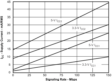
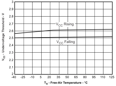
7.22 Typical Characteristics
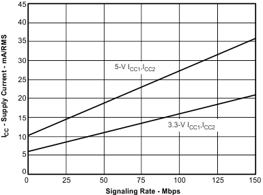
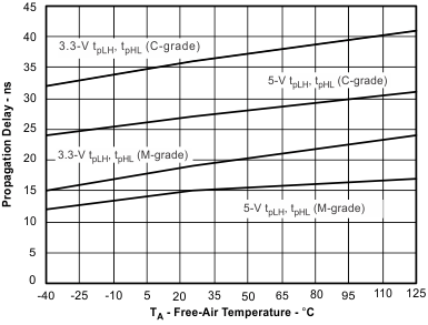
| TA = 25°C | Load = 15 pF | All Channels |
Signaling Rate
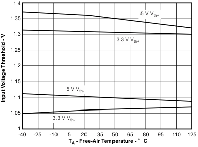
| Air Flow at 7 cf/m | Low_K Board |
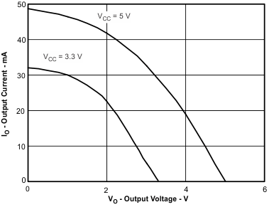
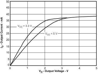
| TA = 25°C | Load = 15 pF |
High-Level Output Voltage
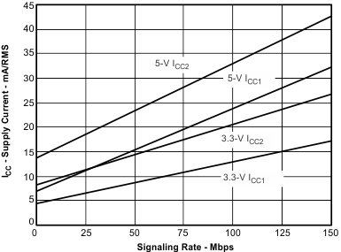
| TA = 25°C | Load = 15 pF | All Channels |
Signaling Rate
| TA = 25°C | Load = 15 pF | All Channels |
| TA = 25°C | Load = 15 pF |
Low-Level Output Voltage
