SLLSEC3F September 2012 – April 2016 ISO7631FC , ISO7631FM , ISO7641FC
PRODUCTION DATA.
- 1 Features
- 2 Applications
- 3 Description
- 4 Revision History
- 5 Pin Configuration and Functions
-
6 Specifications
- 6.1 Absolute Maximum Ratings
- 6.2 ESD Ratings
- 6.3 Recommended Operating Conditions
- 6.4 Thermal Information
- 6.5 Electrical Characteristics: VCC1 and VCC2 at 5 V ± 10%
- 6.6 Electrical Characteristics: VCC1 at 5 V ± 10% and VCC2 at 3.3 V ± 10%
- 6.7 Electrical Characteristics: VCC1 at 3.3 V ± 10% and VCC2 at 5 V ± 10%
- 6.8 Electrical Characteristics: VCC1 and VCC2 at 3.3 V ± 10%
- 6.9 Electrical Characteristics: VCC1 and VCC2 at 2.7 V (ISO7631FM Only)
- 6.10 Power Dissipation Characteristics
- 6.11 Supply Current Characteristics: VCC1 and VCC2 at 5 V ± 10%
- 6.12 Supply Current Characteristics: VCC1 at 5 V ± 10% and VCC2 at 3.3 V ± 10%
- 6.13 Supply Current Characteristics: VCC1 at 3.3 V ± 10% and VCC2 at 5 V ± 10%
- 6.14 Supply Current Characteristics: VCC1 and VCC2 at 3.3 V ± 10%
- 6.15 Supply Current Characteristics: VCC1 and VCC2 at 2.7 V (ISO7631FM Only) Only M-Grade devices are recommended for operation down to 2.7 V supplies. For 2.7 V-operation, max data rate is 100 Mbps.
- 6.16 Switching Characteristics: VCC1 and VCC2 at 5 V ± 10%
- 6.17 Switching Characteristics: VCC1 at 5 V ± 10% and VCC2 at 3.3 V ± 10%
- 6.18 Switching Characteristics: VCC1 at 3.3 V ± 10% and VCC2 at 5 V ± 10%
- 6.19 Switching Characteristics: VCC1 and VCC2 at 3.3 V ± 10%
- 6.20 Switching Characteristics: VCC1 and VCC2 at 2.7 V Only M-Grade devices are recommended for operation down to 2.7 V supplies. For 2.7 V-operation, max data rate is 100 Mbps.
- 6.21 Typical Characteristics
- 7 Parameter Measurement Information
- 8 Detailed Description
- 9 Application and Implementation
- 10Power Supply Recommendations
- 11Layout
- 12Device and Documentation Support
- 13Mechanical, Packaging, and Orderable Information
Package Options
Refer to the PDF data sheet for device specific package drawings
Mechanical Data (Package|Pins)
- DW|16
Thermal pad, mechanical data (Package|Pins)
Orderable Information
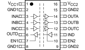
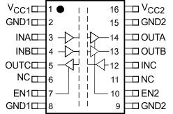
5 Pin Configuration and Functions
ISO7641 DW Package
16-Pin SOIC
Top View

Pin Functions
| PIN | I/O | DESCRIPTION | ||
|---|---|---|---|---|
| NAME | ISO7641 | ISO7631 | ||
| EN1 | 7 | 7 | I | Enables (when input is High or Open) or Disables (when input is Low) OUTD of ISO7641 and OUTC of ISO7631 |
| EN2 | 10 | 10 | I | Enables (when input is High or Open) or Disables (when input is Low) OUTA, OUTB, and OUTC of ISO7641 Enables (when input is High or Open) or Disables (when input is Low) OUTA and OUTB of ISO7631 |
| GND1 | 2, 8 | 2, 8 | – | Ground connection for VCC1 |
| GND2 | 9, 15 | 9, 15 | – | Ground connection for VCC2 |
| INA | 3 | 3 | I | Input, channel A |
| INB | 4 | 4 | I | Input, channel B |
| INC | 5 | 12 | I | Input, channel C |
| IND | 11 | – | I | Input, channel D |
| NC | – | 6,11 | – | No Connect pins are floating with no internal connection |
| OUTA | 14 | 14 | O | Output, channel A |
| OUTB | 13 | 13 | O | Output, channel B |
| OUTC | 12 | 5 | O | Output, channel C |
| OUTD | 6 | – | O | Output, channel D |
| VCC1 | 1 | 1 | – | Power supply, VCC1 |
| VCC2 | 16 | 16 | – | Power supply, VCC2 |
