SNVSBF7 November 2019 LDC1001
PRODUCTION DATA.
- 1 Features
- 2 Applications
- 3 Description
- 4 Revision History
- 5 Pin Configuration and Functions
- 6 Specifications
-
7 Detailed Description
- 7.1 Overview
- 7.2 Functional Block Diagram
- 7.3 Feature Description
- 7.4 Device Functional Modes
- 7.5 Programming
- 7.6
Register Maps
- 7.6.1
Register Description
- 7.6.1.1 Revision ID (Address = 0x00)
- 7.6.1.2 RP_MAX (Address = 0x01)
- 7.6.1.3 RP_MIN (Address = 0x02)
- 7.6.1.4 Watchdog Timer Frequency (Address = 0x03)
- 7.6.1.5 LDC Configuration (Address = 0x04)
- 7.6.1.6 Clock Configuration (Address = 0x05)
- 7.6.1.7 Comparator Threshold High LSB (Address = 0x06)
- 7.6.1.8 Comparator Threshold High MSB (Address = 0x07)
- 7.6.1.9 Comparator Threshold Low LSB (Address = 0x08)
- 7.6.1.10 Comparator Threshold Low MSB (Address = 0x09)
- 7.6.1.11 INTB Pin Configuration (Address = 0x0A)
- 7.6.1.12 Power Configuration (Address = 0x0B)
- 7.6.1.13 Status (Address = 0x20)
- 7.6.1.14 Proximity Data LSB (Address = 0x21)
- 7.6.1.15 Proximity Data MSB (Address = 0x22)
- 7.6.1.16 Frequency Counter LSB (Address = 0x23)
- 7.6.1.17 Frequency Counter Mid-Byte (Address = 0x24)
- 7.6.1.18 Frequency Counter MSB (Address = 0x25)
- 7.6.1
Register Description
- 8 Application and Implementation
- 9 Power Supply Recommendations
- 10Layout
- 11Device and Documentation Support
- 12Mechanical, Packaging, and Orderable Information
Package Options
Mechanical Data (Package|Pins)
- NHR|16
Thermal pad, mechanical data (Package|Pins)
Orderable Information
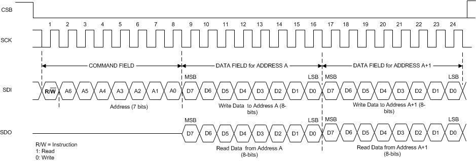
7.5.1.1 Extended SPI Transactions
A SPI transaction may be extended to multiple registers by keeping the CSB asserted for more than 16 pulses on SCLK. In this mode, the register addresses increment automatically. CSB must be remain asserted during 8*(1+N) clock cycles of SCLK, where N is the amount of bytes to write or read during the transaction.
During an extended read access, SDO outputs the register contents every 8 clock cycles after the initial 8 clocks of the command field. During an extended write access, the data is written to the registers every 8 clock cycles after the initial 8 clocks of the command field.
Extended transactions can be used to read 16 bits of proximity data and 24 bits of frequency data all in one SPI transaction by initiating a read from register 0x21.
 Figure 16. Extended SPI Transaction