SNVSBF7 November 2019 LDC1001
PRODUCTION DATA.
- 1 Features
- 2 Applications
- 3 Description
- 4 Revision History
- 5 Pin Configuration and Functions
- 6 Specifications
-
7 Detailed Description
- 7.1 Overview
- 7.2 Functional Block Diagram
- 7.3 Feature Description
- 7.4 Device Functional Modes
- 7.5 Programming
- 7.6
Register Maps
- 7.6.1
Register Description
- 7.6.1.1 Revision ID (Address = 0x00)
- 7.6.1.2 RP_MAX (Address = 0x01)
- 7.6.1.3 RP_MIN (Address = 0x02)
- 7.6.1.4 Watchdog Timer Frequency (Address = 0x03)
- 7.6.1.5 LDC Configuration (Address = 0x04)
- 7.6.1.6 Clock Configuration (Address = 0x05)
- 7.6.1.7 Comparator Threshold High LSB (Address = 0x06)
- 7.6.1.8 Comparator Threshold High MSB (Address = 0x07)
- 7.6.1.9 Comparator Threshold Low LSB (Address = 0x08)
- 7.6.1.10 Comparator Threshold Low MSB (Address = 0x09)
- 7.6.1.11 INTB Pin Configuration (Address = 0x0A)
- 7.6.1.12 Power Configuration (Address = 0x0B)
- 7.6.1.13 Status (Address = 0x20)
- 7.6.1.14 Proximity Data LSB (Address = 0x21)
- 7.6.1.15 Proximity Data MSB (Address = 0x22)
- 7.6.1.16 Frequency Counter LSB (Address = 0x23)
- 7.6.1.17 Frequency Counter Mid-Byte (Address = 0x24)
- 7.6.1.18 Frequency Counter MSB (Address = 0x25)
- 7.6.1
Register Description
- 8 Application and Implementation
- 9 Power Supply Recommendations
- 10Layout
- 11Device and Documentation Support
- 12Mechanical, Packaging, and Orderable Information
Package Options
Mechanical Data (Package|Pins)
- NHR|16
Thermal pad, mechanical data (Package|Pins)
Orderable Information
7.3.2 Measuring RP With LDC1001
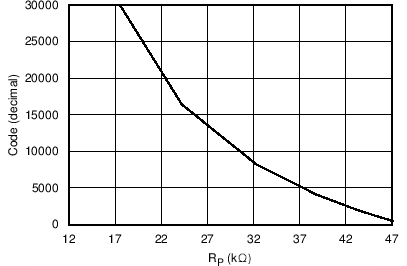
The LDC1001 supports a wide range of LC combinations, with oscillation frequencies ranging from 5 kHz to 5 MHz and RP ranging from 798 Ω to 3.93 MΩ. This range of RP can be viewed as the maximum input range of an ADC. As shown in Figure 9, the range of RP is typically much smaller than the maximum input range supported by the LDC1001. To get better resolution in the desired sensing range, the LDC1001 offers a programmable input range through the RP_MIN and RP_MAX registers. Refer to Calculation of RP_MIN and RP_MAX for information on setting these registers.
When the resonance impedance RP of the sensor drops below the programed RP_MIN, the RP output of the LDC will clip at its full scale output. This situation could, for example, happen when a target comes too close to the coil.
 Figure 10. Transfer Characteristics of LDC1001 With RP_MIN = 16.160 kΩ and RP_MAX = 48.481 kΩ
 Use Equation 2 to calculate the resonance impedance from the digital output code:

where
- RP = Measured sensor parallel resistance in kΩ.
- RP_MIN is the resistance (in kΩ) selected in register 0x02
- RP_MAX is the resistance (in kΩ) selected in register 0x01
- Y = Proximity Data÷215
- Proximity data is the LDC RP output = (Contents of Register 0x22) × 28 + (Contents of register 0x21).
Example: If Proximity data (address 0x22:0x21) is 5000, RP_MIN is 2.394 kΩ, and RP_MAX is 38.785 kΩ ,the resonance impedance is given by:
Y = 5000/215 = 0.1526
RP = (38785 × 2394) ÷ (2394 × (1 – 0.1526) + 38785 × 0.1526) = (92851290 ÷ (2028.675 + 5918.591))
RP = 11.683 kΩ