SNOSCZ0A December   2014  – March 2018 LDC1312 , LDC1314

PRODUCTION DATA.  

  1. Features
  2. Applications
  3. Description
    1.     Device Images
      1.      Simplified Schematic
      2.      Measurement Precision vs. Target Distance
  4. Revision History
  5. Pin Configuration and Functions
    1.     Pin Functions
  6. Specifications
    1. 6.1 Absolute Maximum Ratings
    2. 6.2 ESD Ratings
    3. 6.3 Recommended Operating Conditions
    4. 6.4 Thermal Information
    5. 6.5 Electrical Characteristics
    6. 6.6 Switching Characteristics - I2C
    7. 6.7 Typical Characteristics
  7. Detailed Description
    1. 7.1 Overview
    2. 7.2 Functional Block Diagram
    3. 7.3 Feature Description
      1. 7.3.1 Multi-Channel and Single Channel Operation
      2. 7.3.2 Adjustable Conversion Time
      3. 7.3.3 Digital Signal Gain
      4. 7.3.4 Sensor Startup and Glitch Configuration
      5. 7.3.5 Reference Clock
      6. 7.3.6 Sensor Current Drive Control
      7. 7.3.7 Device Status Monitoring
    4. 7.4 Device Functional Modes
      1. 7.4.1 Startup Mode
      2. 7.4.2 Sleep Mode (Configuration Mode)
      3. 7.4.3 Normal (Conversion) Mode
      4. 7.4.4 Shutdown Mode
        1. 7.4.4.1 Reset
    5. 7.5 Programming
      1. 7.5.1 I2C Interface Specifications
      2. 7.5.2 Pulses on I2C
    6. 7.6 Register Maps
      1. 7.6.1  Register List
      2. 7.6.2  Address 0x00, DATA0
        1. Table 1. Address 0x00, DATA0 Field Descriptions
      3. 7.6.3  Address 0x02, DATA1
        1. Table 2. Address 0x02, DATA1 Field Descriptions
      4. 7.6.4  Address 0x04, DATA2 (LDC1314 only)
        1. Table 3. Address 0x04, DATA2 Field Descriptions
      5. 7.6.5  Address 0x06, DATA3 (LDC1314 only)
        1. Table 4. Address 0x06, DATA3 Field Descriptions
      6. 7.6.6  Address 0x08, RCOUNT0
        1. Table 5. Address 0x08, RCOUNT0 Field Descriptions
      7. 7.6.7  Address 0x09, RCOUNT1
        1. Table 6. Address 0x09, RCOUNT1 Field Descriptions
      8. 7.6.8  Address 0x0A, RCOUNT2 (LDC1314 only)
        1. Table 7. Address 0x0A, RCOUNT2 Field Descriptions
      9. 7.6.9  Address 0x0B, RCOUNT3 (LDC1314 only)
        1. Table 8. Address 0x0B, RCOUNT3 Field Descriptions
      10. 7.6.10 Address 0x0C, OFFSET0
        1. Table 9. OFFSET0 Field Descriptions
      11. 7.6.11 Address 0x0D, OFFSET1
        1. Table 10. Address 0x0D, OFFSET1 Field Descriptions
      12. 7.6.12 Address 0x0E, OFFSET2 (LDC1314 only)
        1. Table 11. Address 0x0E, OFFSET2 Field Descriptions
      13. 7.6.13 Address 0x0F, OFFSET3 (LDC1314 only)
        1. Table 12. Address 0x0F, OFFSET3 Field Descriptions
      14. 7.6.14 Address 0x10, SETTLECOUNT0
        1. Table 13. Address 0x10, SETTLECOUNT0 Field Descriptions
      15. 7.6.15 Address 0x11, SETTLECOUNT1
        1. Table 14. Address 0x11, SETTLECOUNT1 Field Descriptions
      16. 7.6.16 Address 0x12, SETTLECOUNT2 (LDC1314 only)
        1. Table 15. Address 0x12, SETTLECOUNT2 Field Descriptions
      17. 7.6.17 Address 0x13, SETTLECOUNT3 (LDC1314 only)
        1. Table 16. Address 0x13, SETTLECOUNT3 Field Descriptions
      18. 7.6.18 Address 0x14, CLOCK_DIVIDERS0
        1. Table 17. Address 0x14, CLOCK_DIVIDERS0 Field Descriptions
      19. 7.6.19 Address 0x15, CLOCK_DIVIDERS1
        1. Table 18. Address 0x15, CLOCK_DIVIDERS1 Field Descriptions
      20. 7.6.20 Address 0x16, CLOCK_DIVIDERS2 (LDC1314 only)
        1. Table 19. Address 0x16, CLOCK_DIVIDERS2 Field Descriptions
      21. 7.6.21 Address 0x17, CLOCK_DIVIDERS3 (LDC1314 only)
        1. Table 20. Address 0x17, CLOCK_DIVIDERS3
      22. 7.6.22 Address 0x18, STATUS
        1. Table 21. Address 0x18, STATUS Field Descriptions
      23. 7.6.23 Address 0x19, ERROR_CONFIG
        1. Table 22. Address 0x19, ERROR_CONFIG
      24. 7.6.24 Address 0x1A, CONFIG
        1. Table 23. Address 0x1A, CONFIG Field Descriptions
      25. 7.6.25 Address 0x1B, MUX_CONFIG
        1. Table 24. Address 0x1B, MUX_CONFIG Field Descriptions
      26. 7.6.26 Address 0x1C, RESET_DEV
        1. Table 25. Address 0x1C, RESET_DEV Field Descriptions
      27. 7.6.27 Address 0x1E, DRIVE_CURRENT0
        1. Table 26. Address 0x1E, DRIVE_CURRENT0 Field Descriptions
      28. 7.6.28 Address 0x1F, DRIVE_CURRENT1
        1. Table 27. Address 0x1F, DRIVE_CURRENT1 Field Descriptions
      29. 7.6.29 Address 0x20, DRIVE_CURRENT2 (LDC1314 only)
        1. Table 28. Address 0x20, DRIVE_CURRENT2 Field Descriptions
      30. 7.6.30 Address 0x21, DRIVE_CURRENT3 (LDC1314 only)
        1. Table 29. DRIVE_CURRENT3 Field Descriptions
      31. 7.6.31 Address 0x7E, MANUFACTURER_ID
        1. Table 30. Address 0x7E, MANUFACTURER_ID Field Descriptions
      32. 7.6.32 Address 0x7F, DEVICE_ID
        1. Table 31. Address 0x7F, DEVICE_ID Field Descriptions
  8. Application and Implementation
    1. 8.1 Application Information
      1. 8.1.1 Conductive Objects in a Time-Varying EM Field
      2. 8.1.2 L-C Resonators
      3. 8.1.3 Multi-Channel and Single Channel Operation
        1. 8.1.3.1 Data Offset
        2. 8.1.3.2 Digital Signal Gain
      4. 8.1.4 Sensor Conversion Time
        1. 8.1.4.1 Settling Time
        2. 8.1.4.2 Sensor Activation
      5. 8.1.5 Sensor Current Drive Configuration
        1. 8.1.5.1 Inactive Channel Sensor Connections
        2. 8.1.5.2 Automatic IDRIVE Setting with RP_OVERRIDE_EN
        3. 8.1.5.3 Determining Sensor IDRIVE for an Unknown Sensor RP Using an Oscilloscope
        4. 8.1.5.4 Sensor Auto-Calibration Mode
        5. 8.1.5.5 Channel 0 High Current Drive
      6. 8.1.6 Clocking Architecture
      7. 8.1.7 Input Deglitch Filter
      8. 8.1.8 Device Status Registers
      9. 8.1.9 Multi-Channel Data Readback
    2. 8.2 Typical Application
      1. 8.2.1 System Sensing Functionality
      2. 8.2.2 Example Application
      3. 8.2.3 Design Requirements
      4. 8.2.4 Detailed Design Procedure
      5. 8.2.5 Recommended Initial Register Configuration Values
      6. 8.2.6 Application Curves
      7. 8.2.7 Inductor Self-Resonant Frequency
  9. Power Supply Recommendations
  10. 10Layout
    1. 10.1 Layout Guidelines
    2. 10.2 Layout Example
  11. 11Device and Documentation Support
    1. 11.1 Device Support
      1. 11.1.1 Development Support
    2. 11.2 Documentation Support
      1. 11.2.1 Related Documentation
    3. 11.3 Related Links
    4. 11.4 Receiving Notification of Documentation Updates
    5. 11.5 Community Resources
    6. 11.6 Trademarks
    7. 11.7 Electrostatic Discharge Caution
    8. 11.8 Glossary
  12. 12Mechanical, Packaging, and Orderable Information

Package Options

Mechanical Data (Package|Pins)
Thermal pad, mechanical data (Package|Pins)
Orderable Information

Multi-Channel Data Readback

When in multi-channel mode, the LDC1312/LDC1314 alternates conversions on all selected channels. After each channel conversion completes, the conversion results for that channel overwrites the previous conversion results with the new data.

When the device completes a conversion on the last channel in the selected group, the device will pull INTB low if DRDY2INT is set to 1. At this time, the conversion results should be retrieved via the I2C bus.

If the device is put into Sleep mode or Shutdown mode, all DATAx registers are cleared of conversion data.
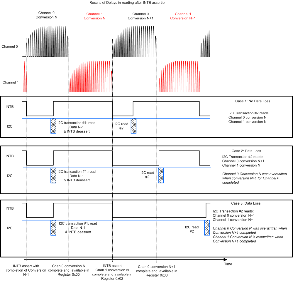
LDC1312 LDC1314 LDC1x1y-data-readback-timing-snoscz0.gifFigure 55. Data Readback Timing

The STATUS register (Address 0x18) flags UNREADCONVx monitor the accesses to the DATAx registers.

When the DATAx register is read, the corresponding UNREADCONVx flag is cleared.

As shown in Figure 55 , if the I2C data readback is delayed, then it is possible to lose older, unread conversion results. Monitoring the UNREADCONVx flags are useful to assess whether data loss is occurring.

A delayed read of previous conversion results can produce the condition in which reading the STATUS register immediately after INTB asserts shows that Channel 0 has no unread data (where the UNREADCONV0 flag is 0), but other channels do have unread data indicated by the corresponding UNREADCONVx flags.