SNOSD68 June 2017 LM10-MIL
PRODUCTION DATA.
- 1 Features
- 2 Applications
- 3 Description
- 4 Revision History
- 5 Pin Configuration and Functions
- 6 Specifications
- 7 Detailed Description
- 8 Application and Implementation
- 9 Power Supply Recommendations
- 10Layout
- 11Device and Documentation Support
- 12Mechanical, Packaging, and Orderable Information
Package Options
Mechanical Data (Package|Pins)
- LMG|8
Thermal pad, mechanical data (Package|Pins)
Orderable Information
8 Application and Implementation
NOTE
Information in the following applications sections is not part of the TI component specification, and TI does not warrant its accuracy or completeness. TI’s customers are responsible for determining suitability of components for their purposes. Customers should validate and test their design implementation to confirm system functionality.
8.1 Application Information
With heavy amplifier loading to V−, resistance drops in the V− lead can adversely affect reference regulation. Lead resistance can approach 1 Ω. Therefore, the common to the reference circuitry should be connected as close as possible to the package.
8.2 Typical Application
8.2.1 Design Requirements
Table 1 lists the design parameters for this example.
Table 1. Design Parameters
| DESIGN PARAMETERS | EXAMPLE VALUE | |||
|---|---|---|---|---|
| Ambient Temperature Range | –55⁰C to 125⁰C | |||
| Supply Voltage Range | 1.2 V to 40 V | |||
| Common-Mode Input Range | (V–) to (V+) – 0.85 V | |||
8.2.2 Detailed Design Procedure
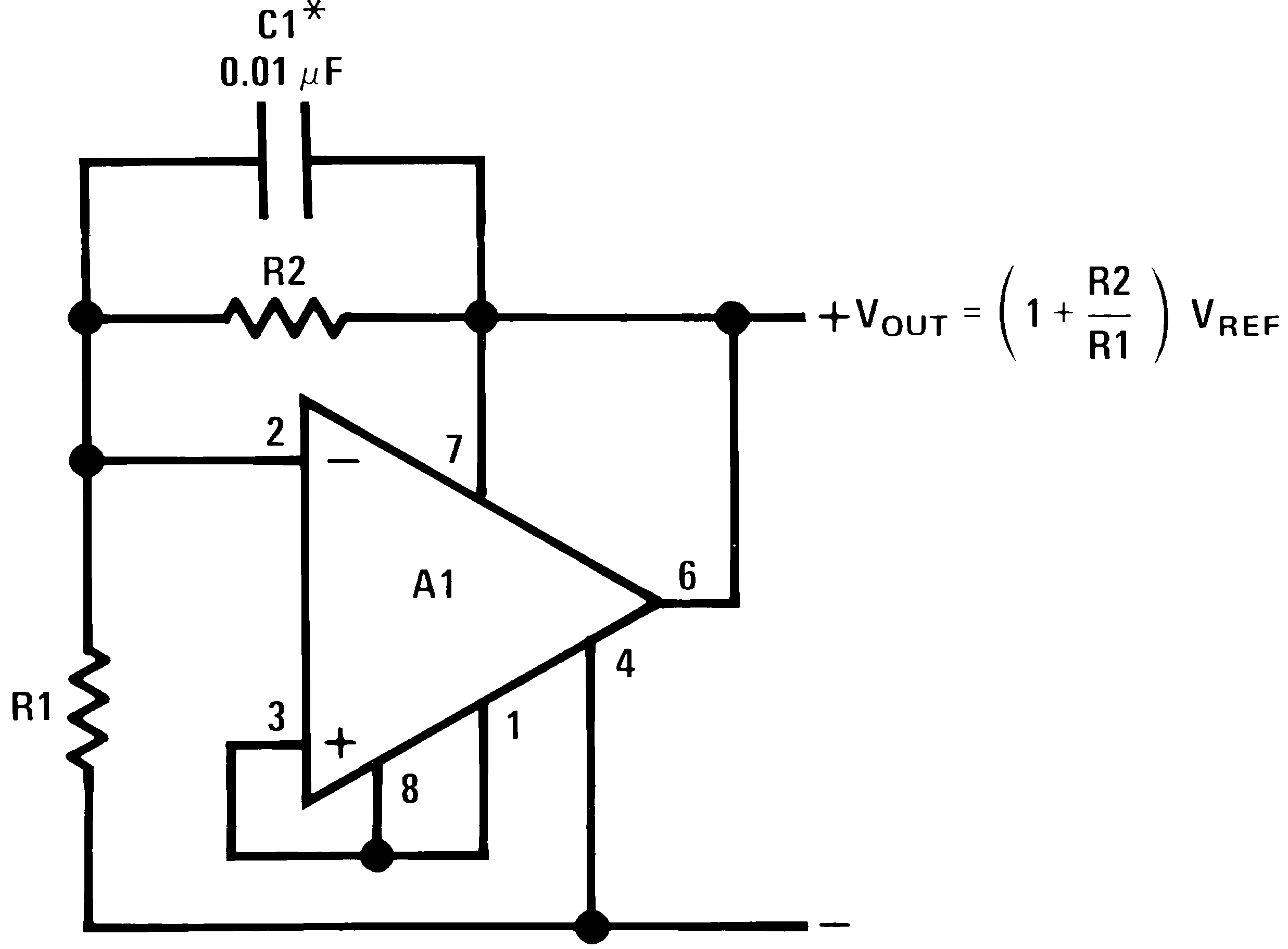
Given that the transfer function of this circuit is:

the output can be set between 0.2 V and the breakdown voltage of the IC by selecting an appropriate value for R2. The circuit regulates for input voltages within a saturation drop of the output (typically 0.4 V at 20 mA and 0.15 V at 5 mA). The regulator is protected from shorts or overloads by current limiting and thermal shutdown.
Typical regulation is about 0.05% load and 0.003%/V line. A substantial improvement in regulation can be effected by connecting the operational amplifier as a follower and setting the reference to the desired output voltage. This has the disadvantage that the minimum input-output differential is increased to a little more than a diode drop. If the operational amplifier were connected for a gain of 2, the output could again saturate. But this requires an additional pair of precision resistors.
The regulator in Figure 36 could be made adjustable to zero by connecting the operational amplifier to a potentiometer on the reference output. This has the disadvantage that the regulation at the lower voltage settings is not as good as it might otherwise be.
8.2.3 Application Curve
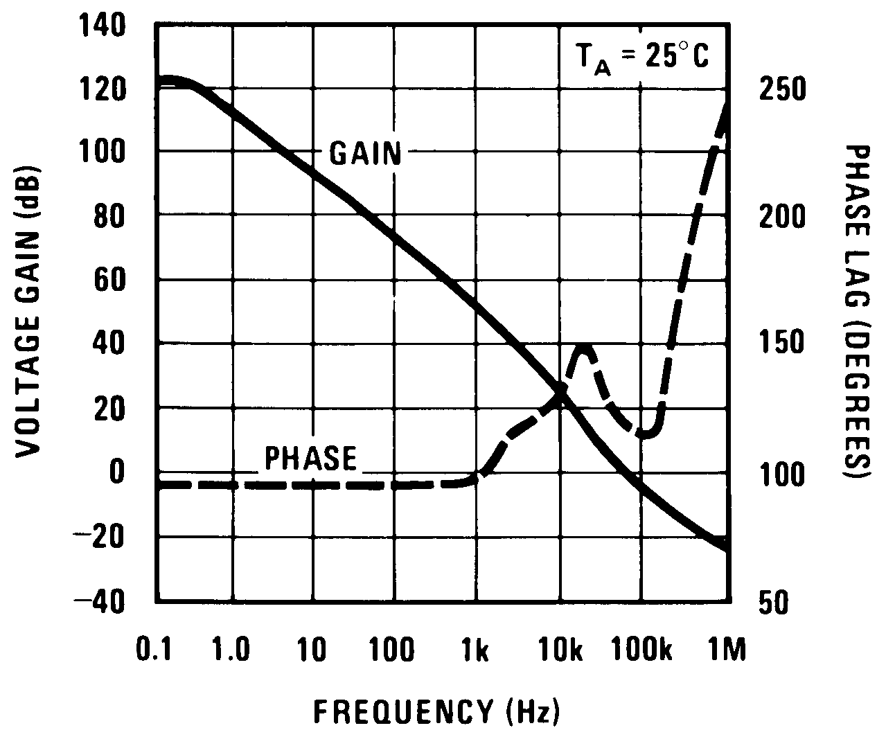 Figure 37. Frequency Response
8.3 System Examples
Circuit descriptions available in application note AN-211 (SNOA638).
8.3.1 Operational Amplifier Offset Adjustment
(Pin numbers are for 8-pin packages)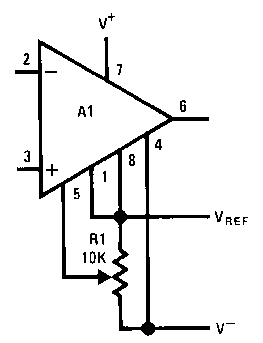 Figure 38. Standard
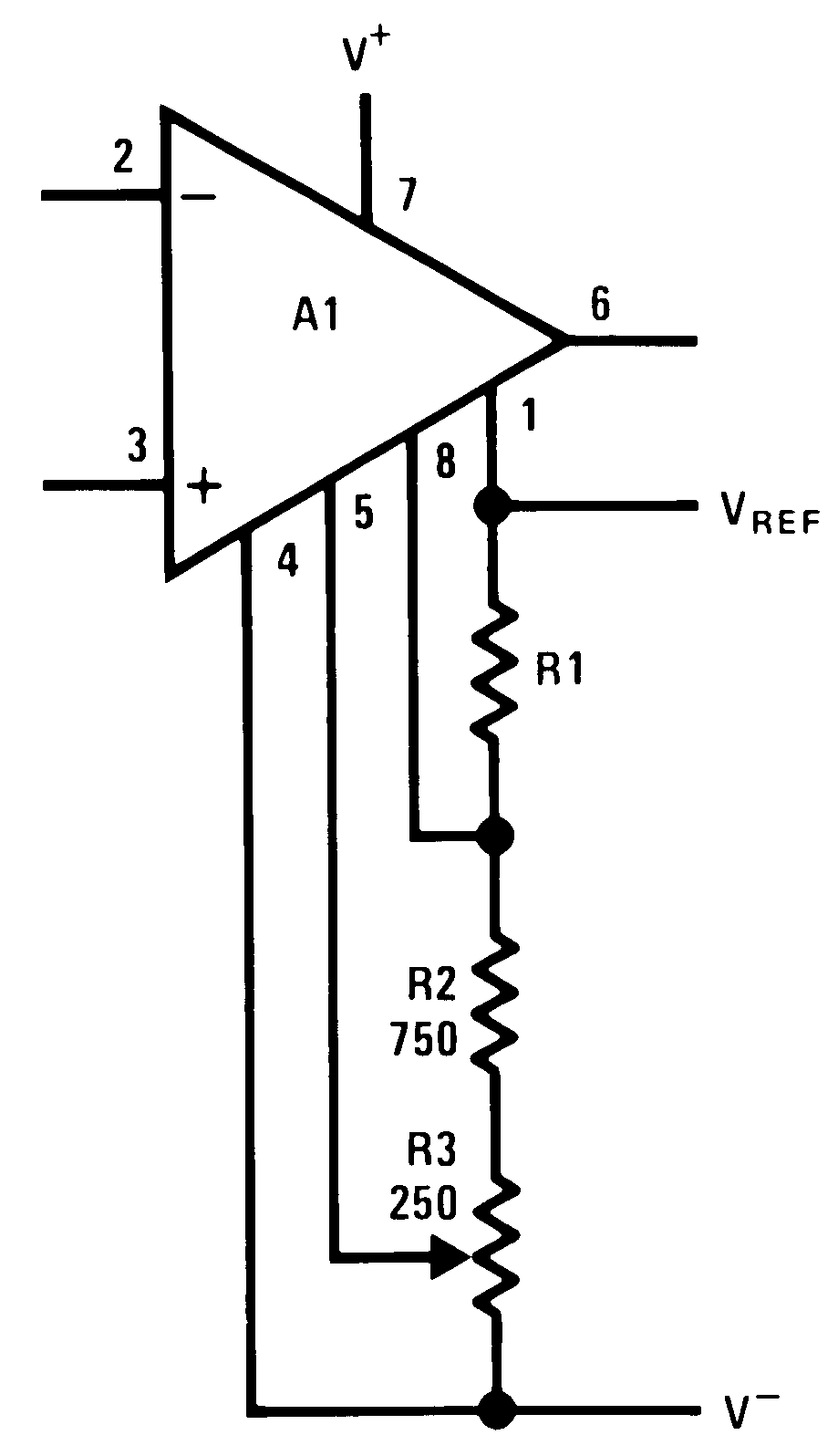 Figure 40. Limited Range With Boosted Reference
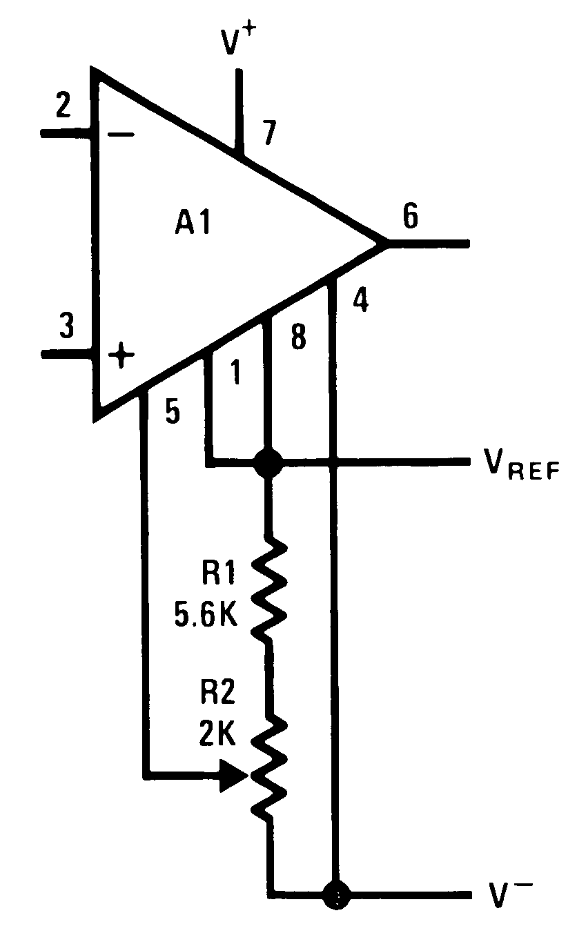 Figure 39. Limited Range
8.3.2 Positive Regulators
(Pin numbers are for 8-pin packages)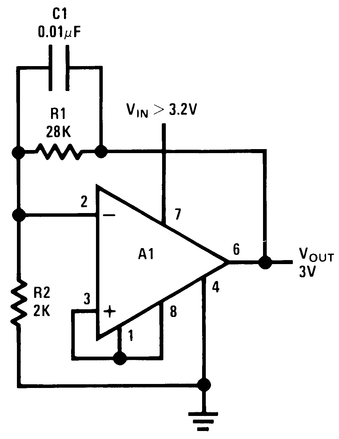 Figure 41. Low Voltage
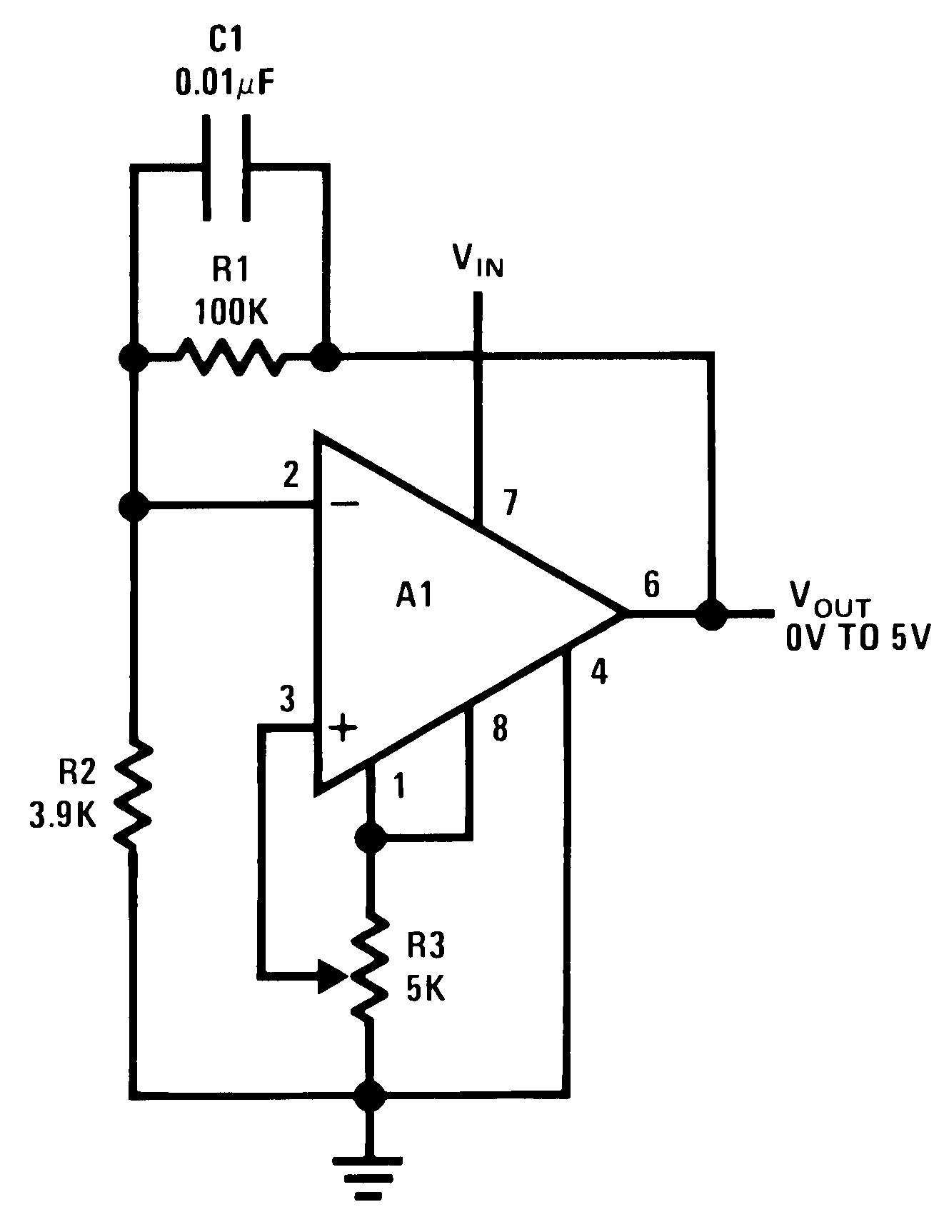
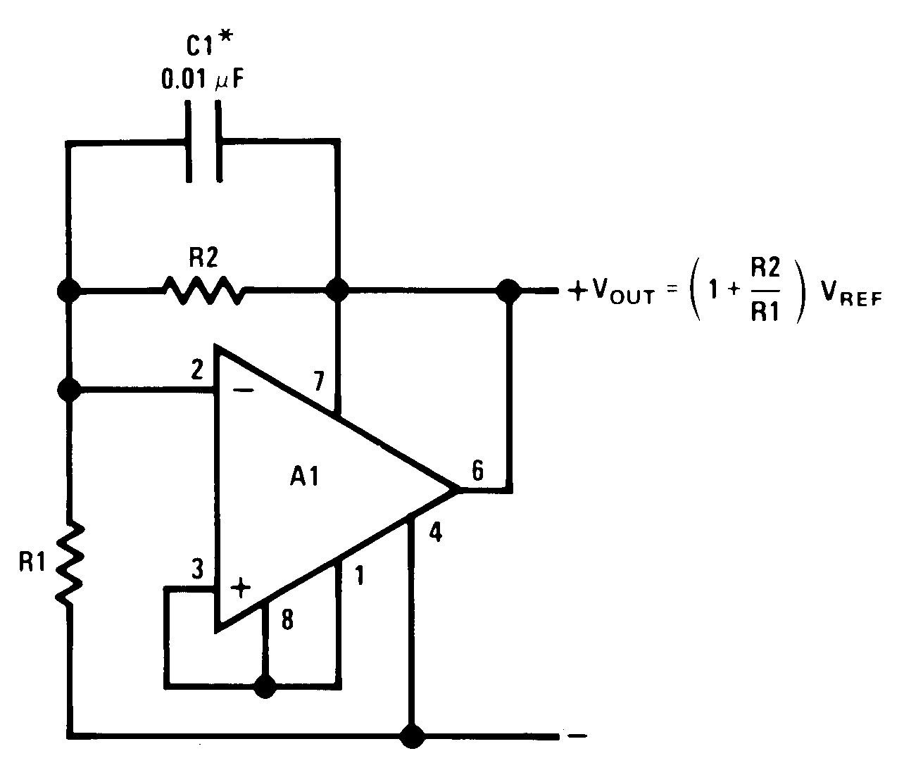
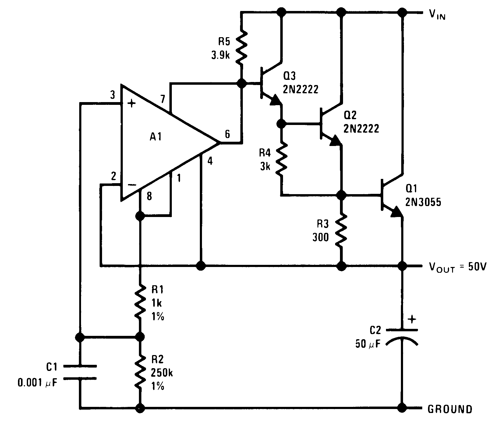 Figure 47. Precision Regulator
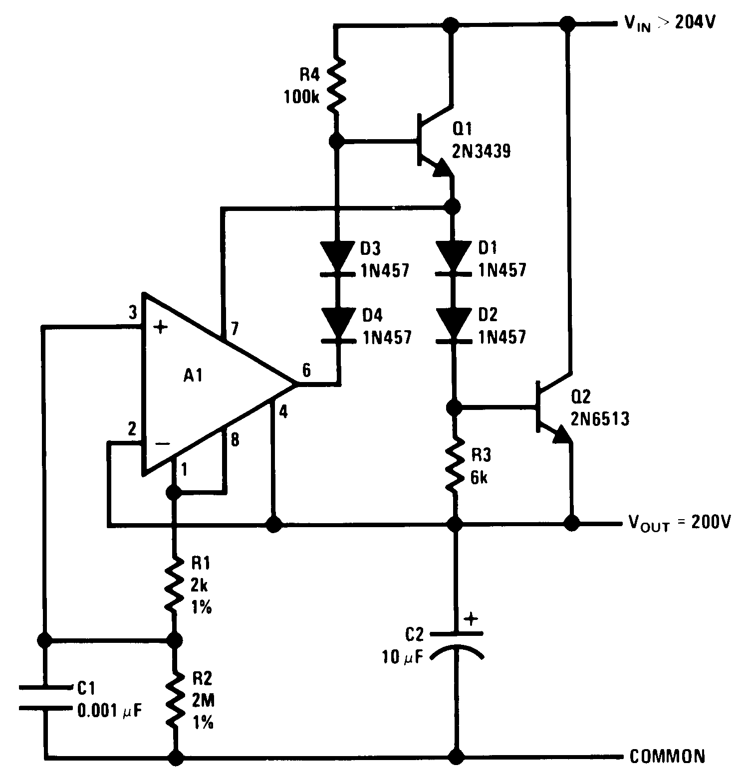
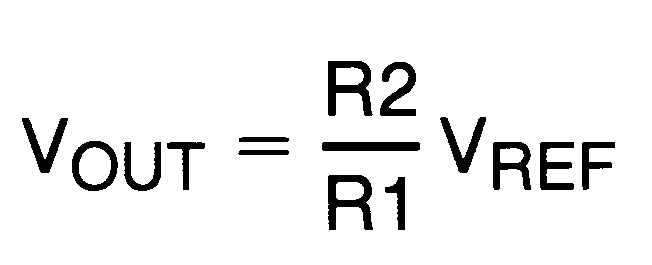

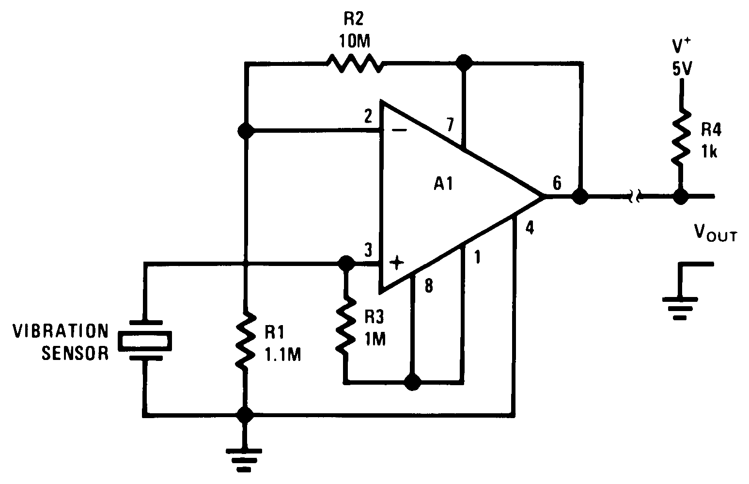 Figure 53. Remote Amplifier
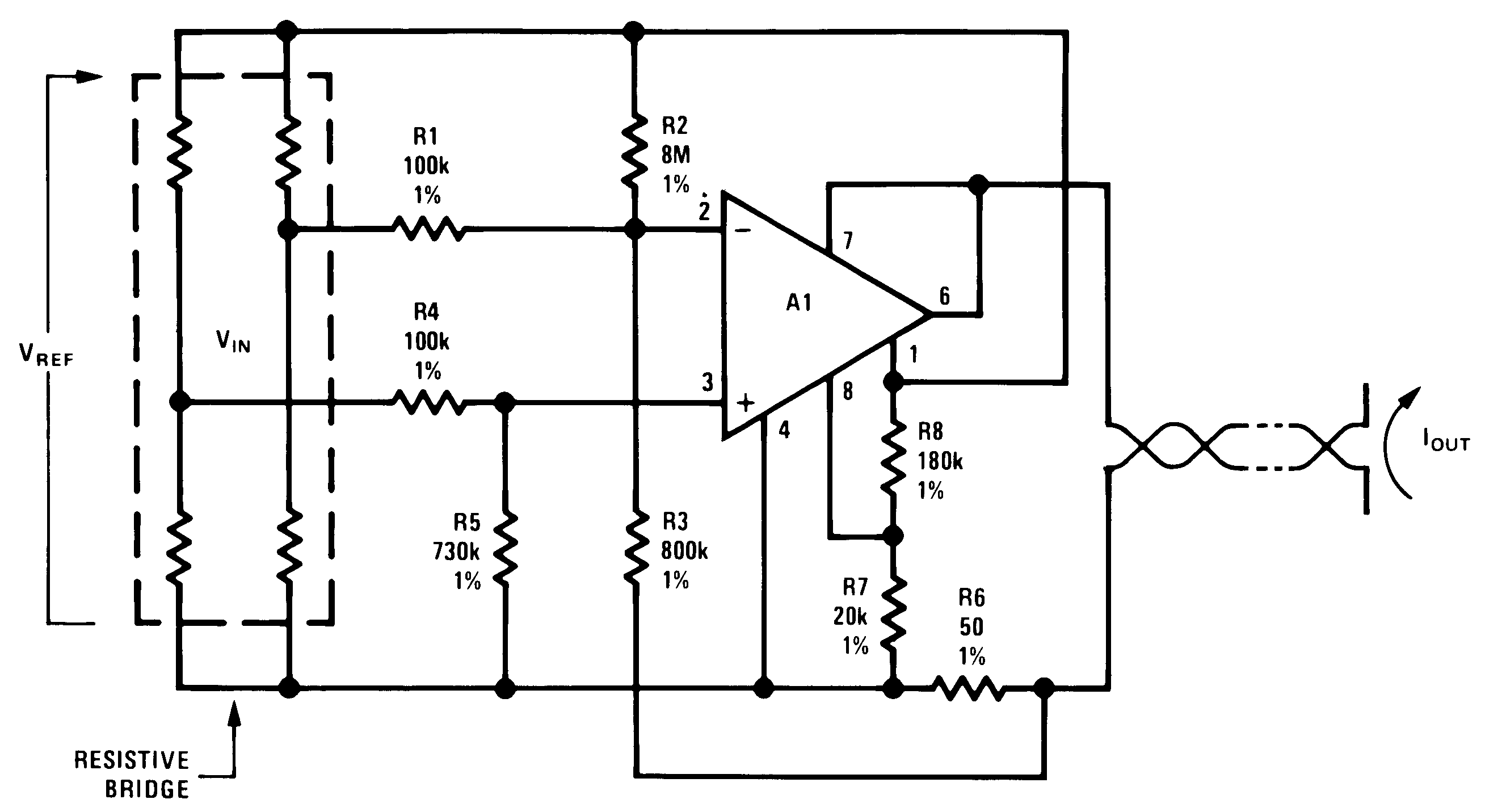 Figure 55. Transmitter for Bridge Sensor
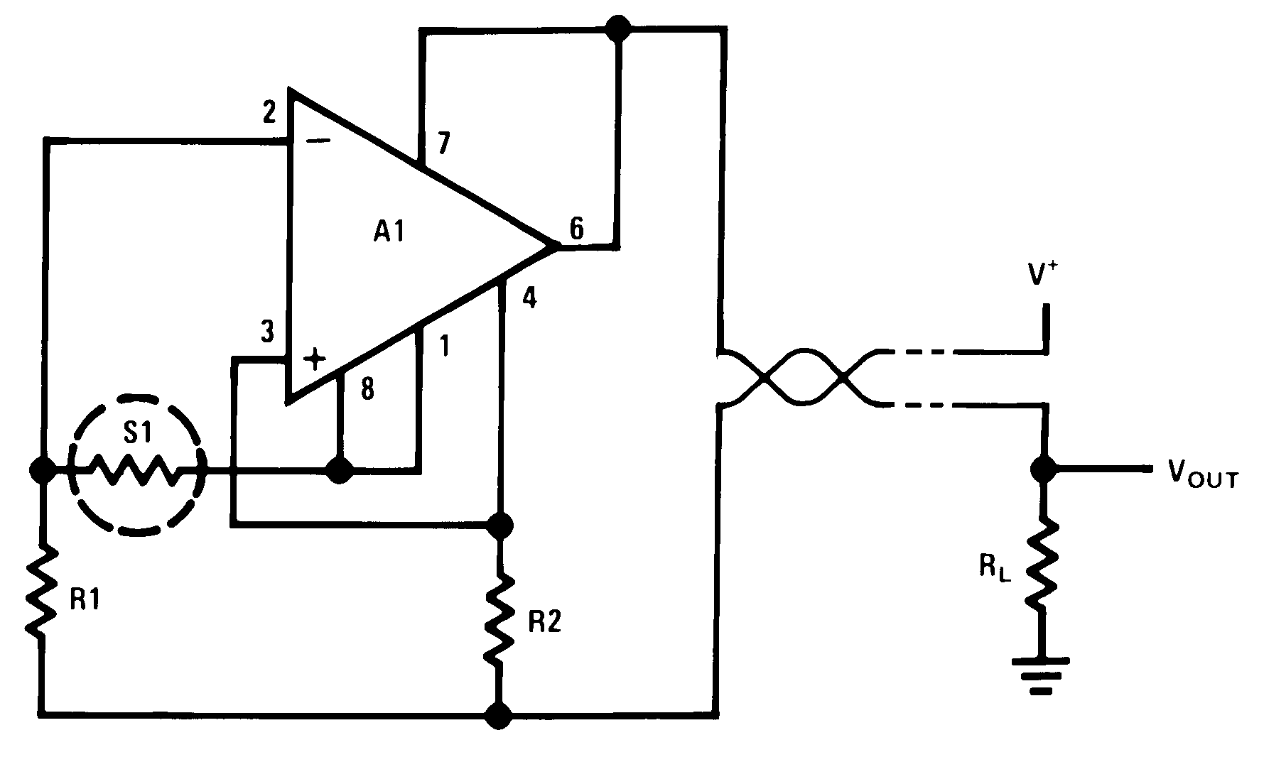 Figure 57. Resistance Thermometer Transmitter
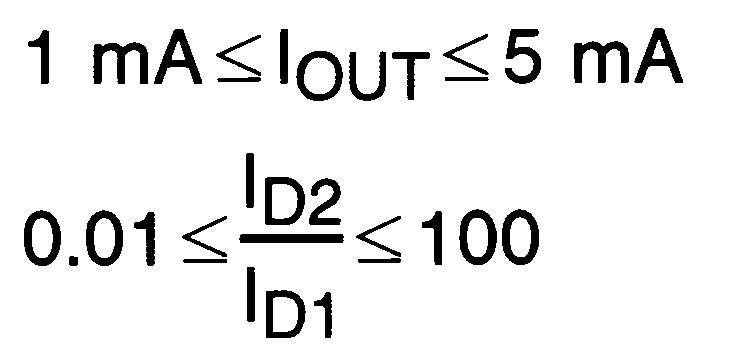
1 mA≤IOUT≤5 mA
†Gain Trim
Transmitter
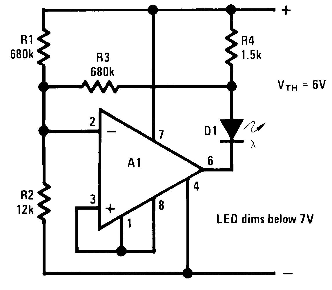 Figure 61. Battery-level Indicator
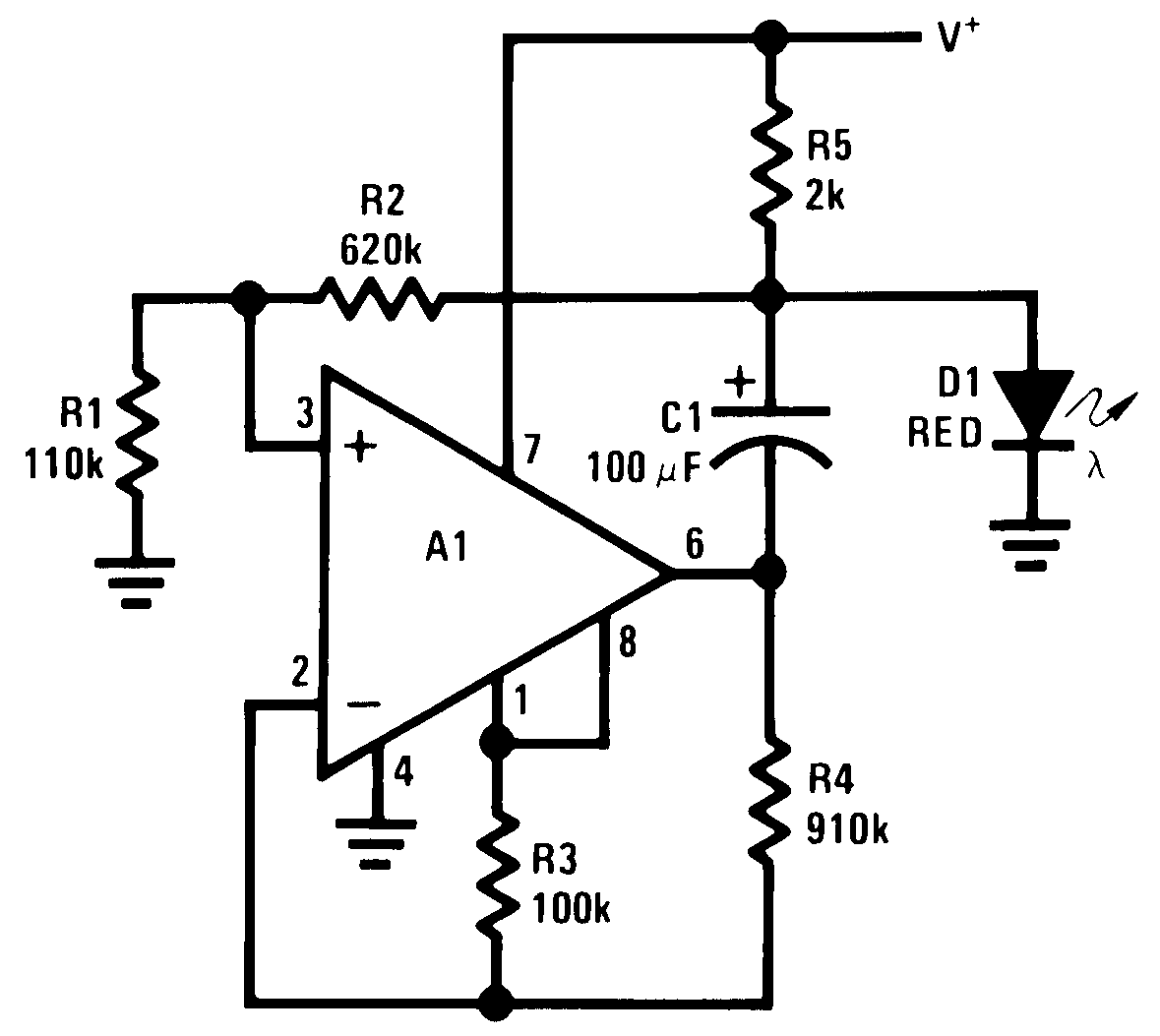
Rate Increases With
Voltage
10 mV, 100nA
FULL-SCALE
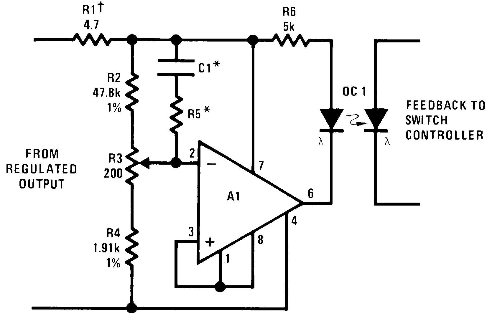
*Optional Frequency Shaping
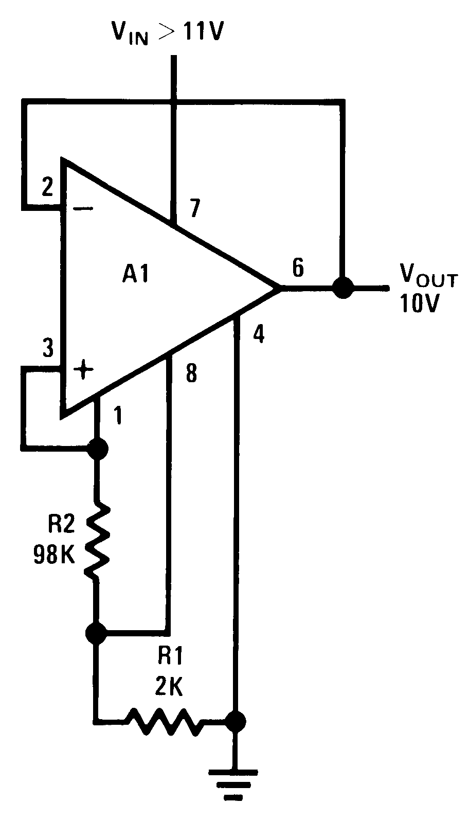 Figure 42. Best Regulation
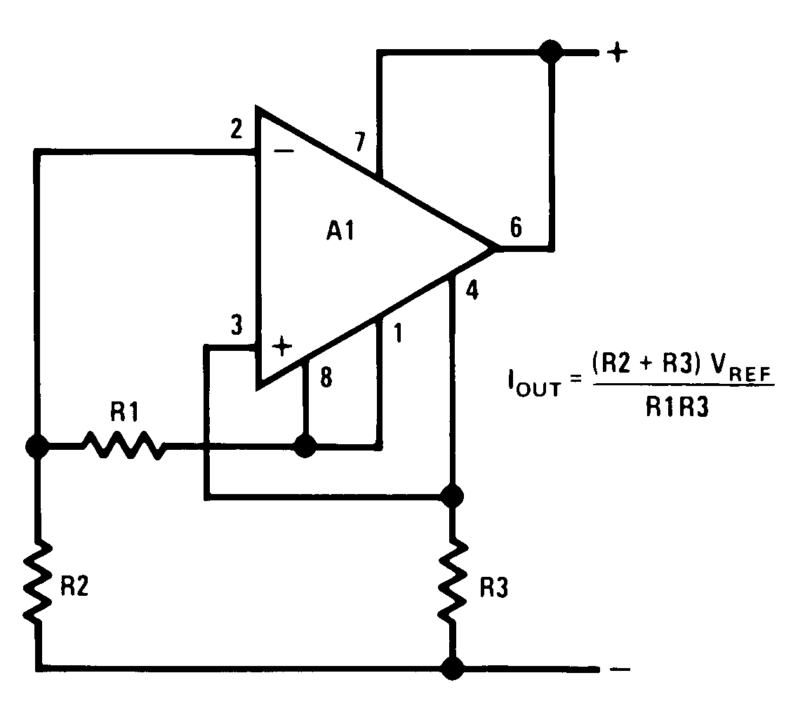 Figure 44. Current Regulator
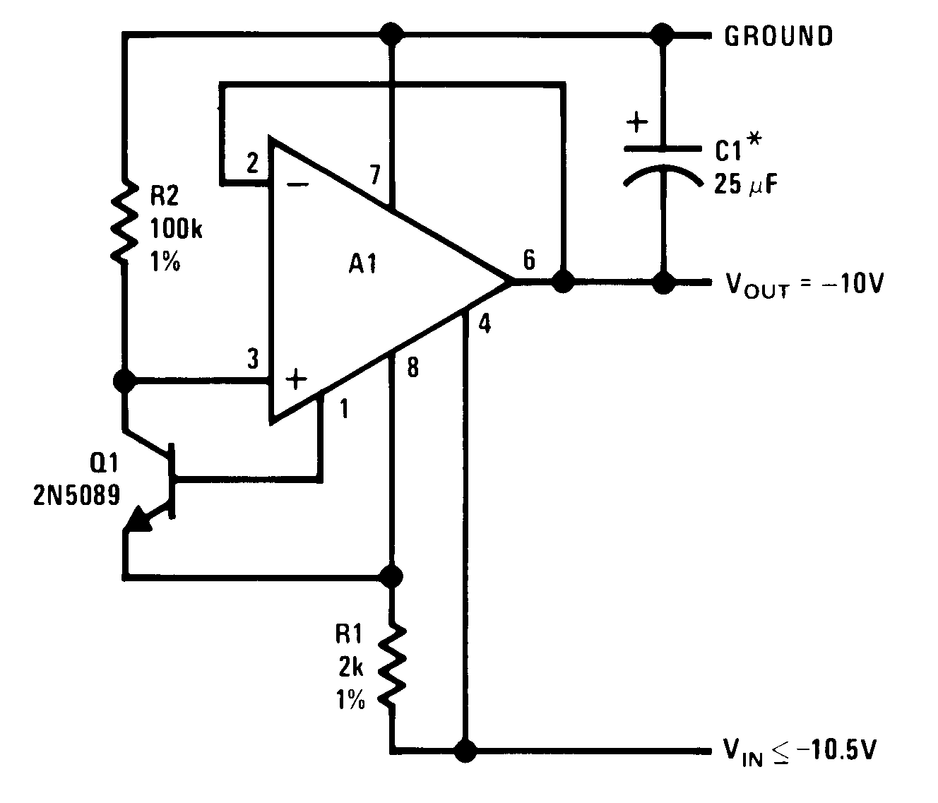
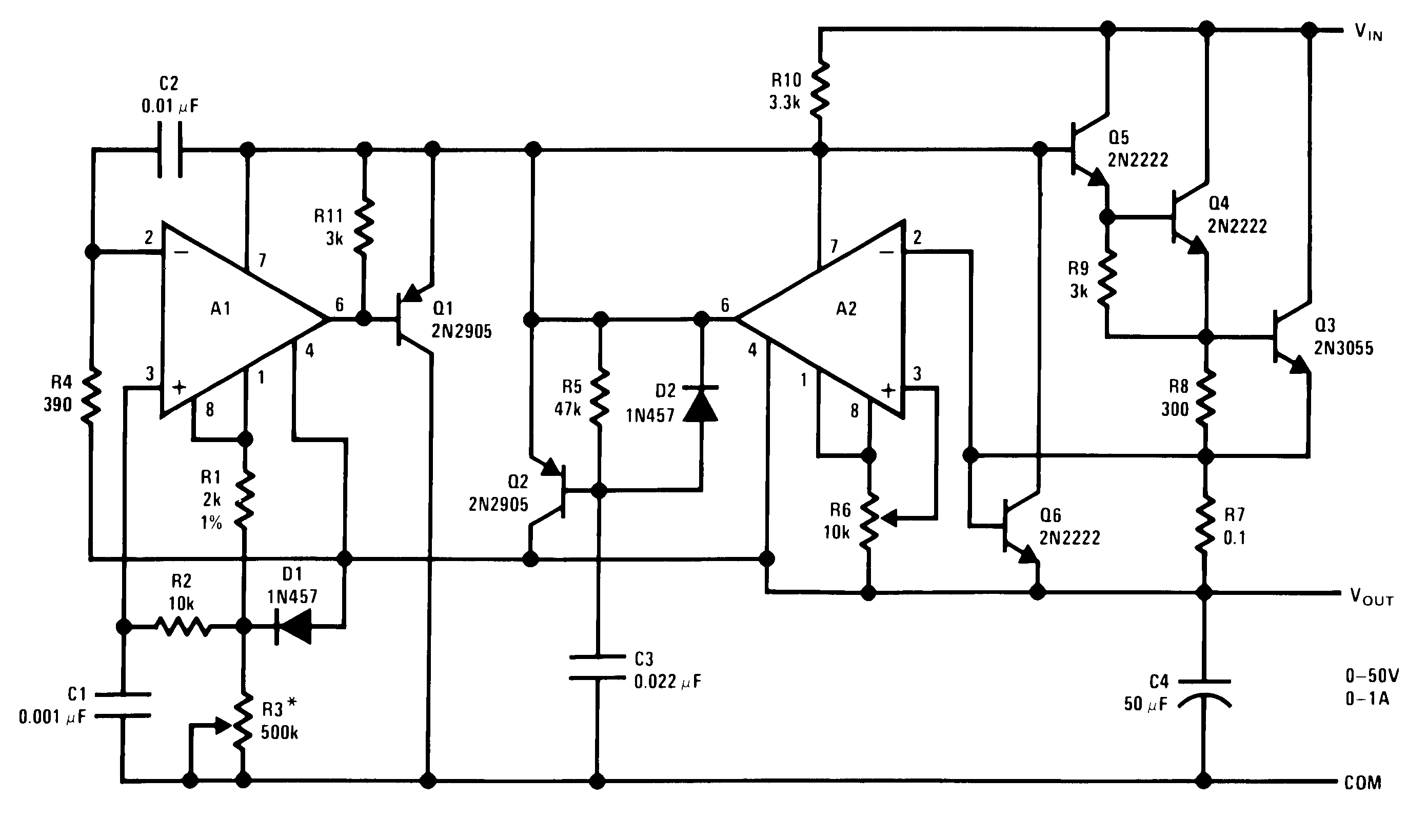
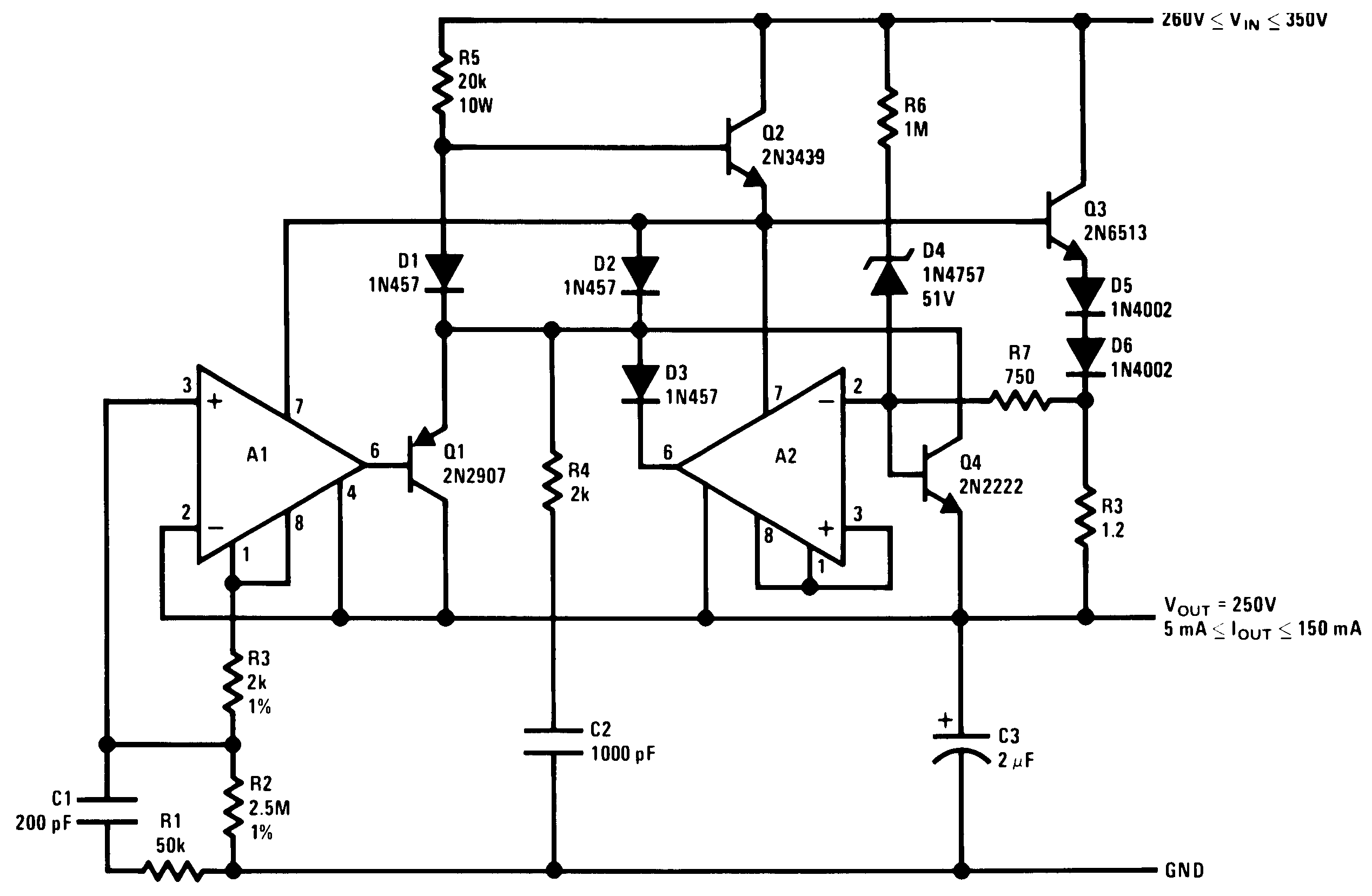 Figure 50. Protected HV Regulator
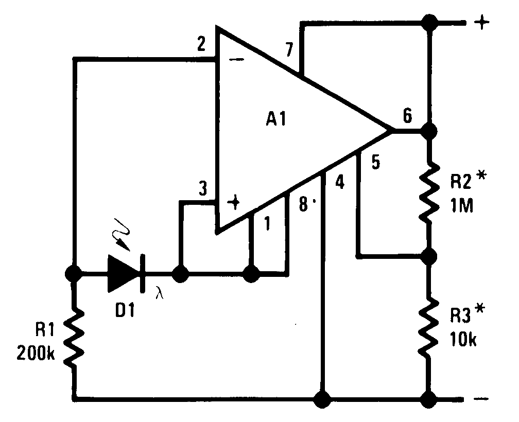
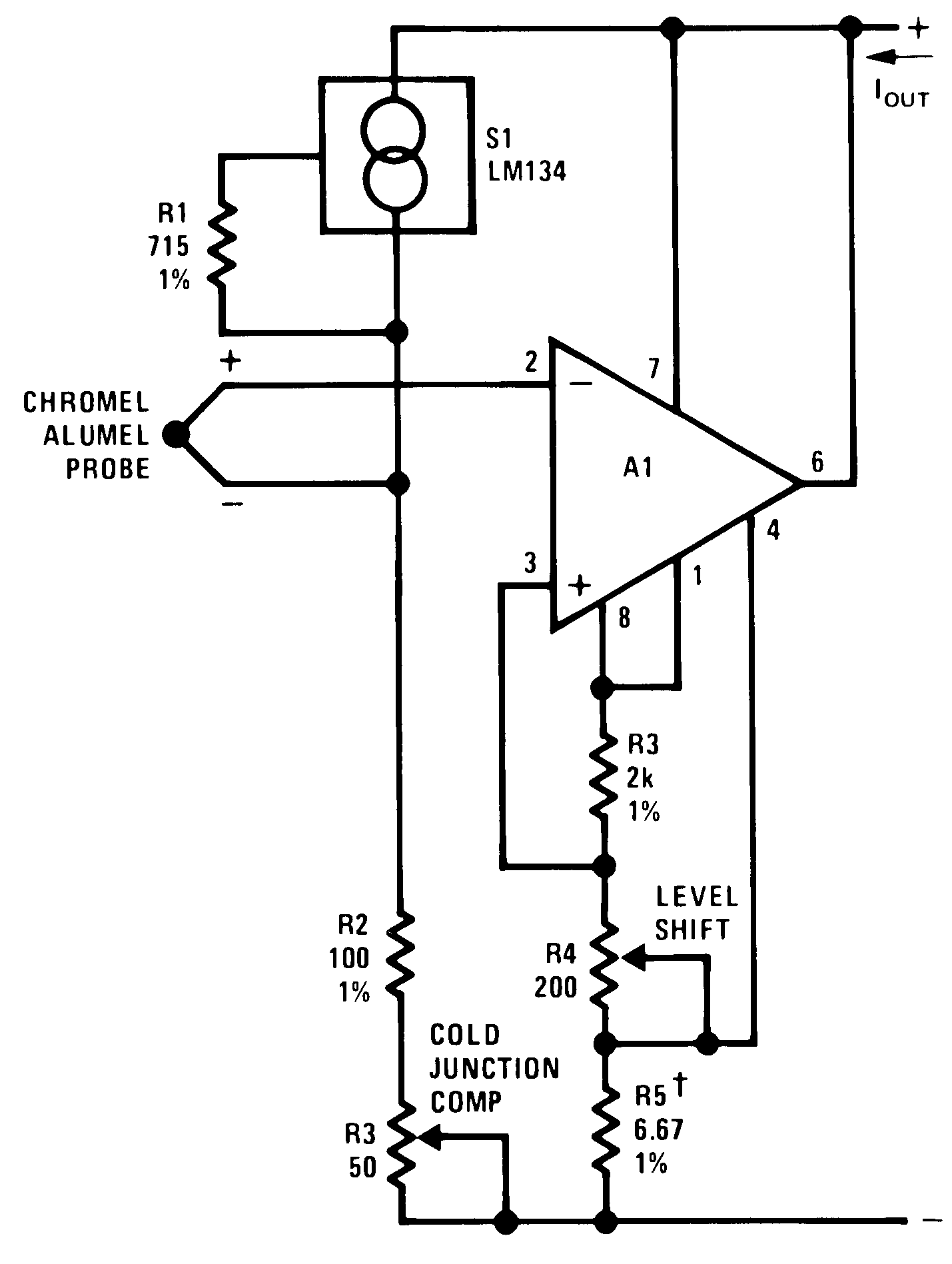
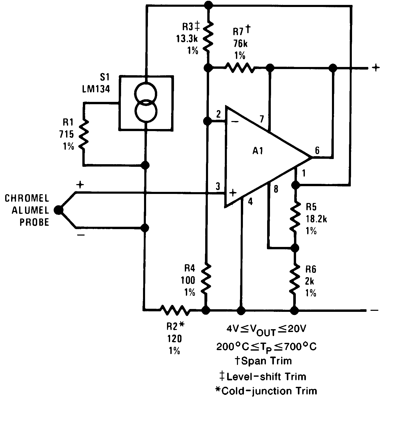 Figure 54. Remote Thermocouple Amplifier
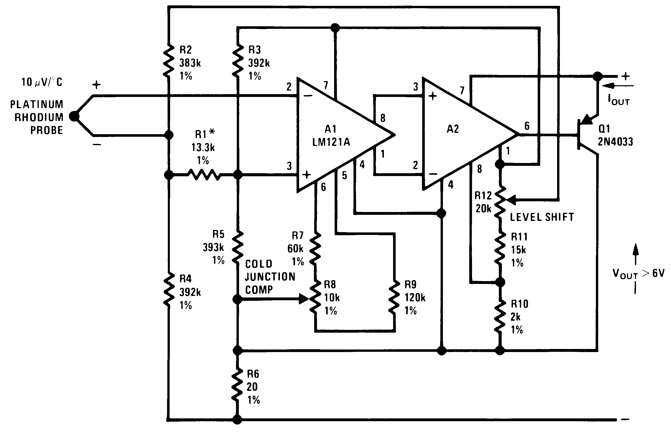
500°C≤TP≤1500°C
*Gain Trim
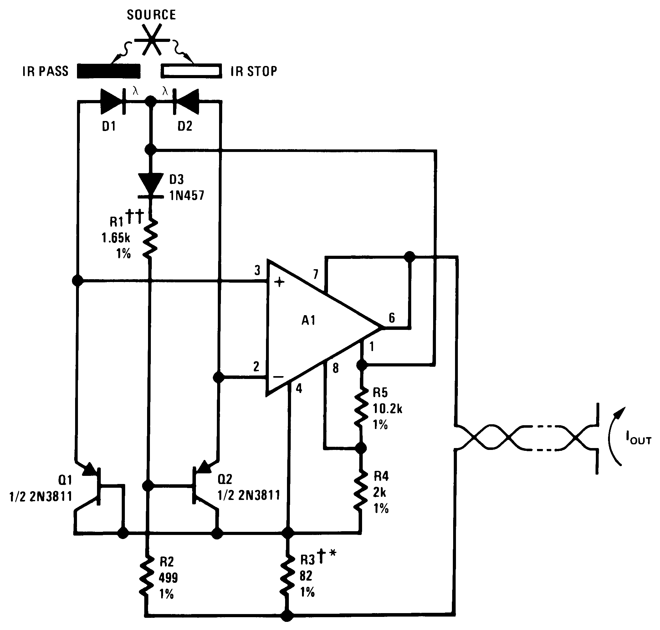
*Scale Factor Trim
†Copper Wire Wound
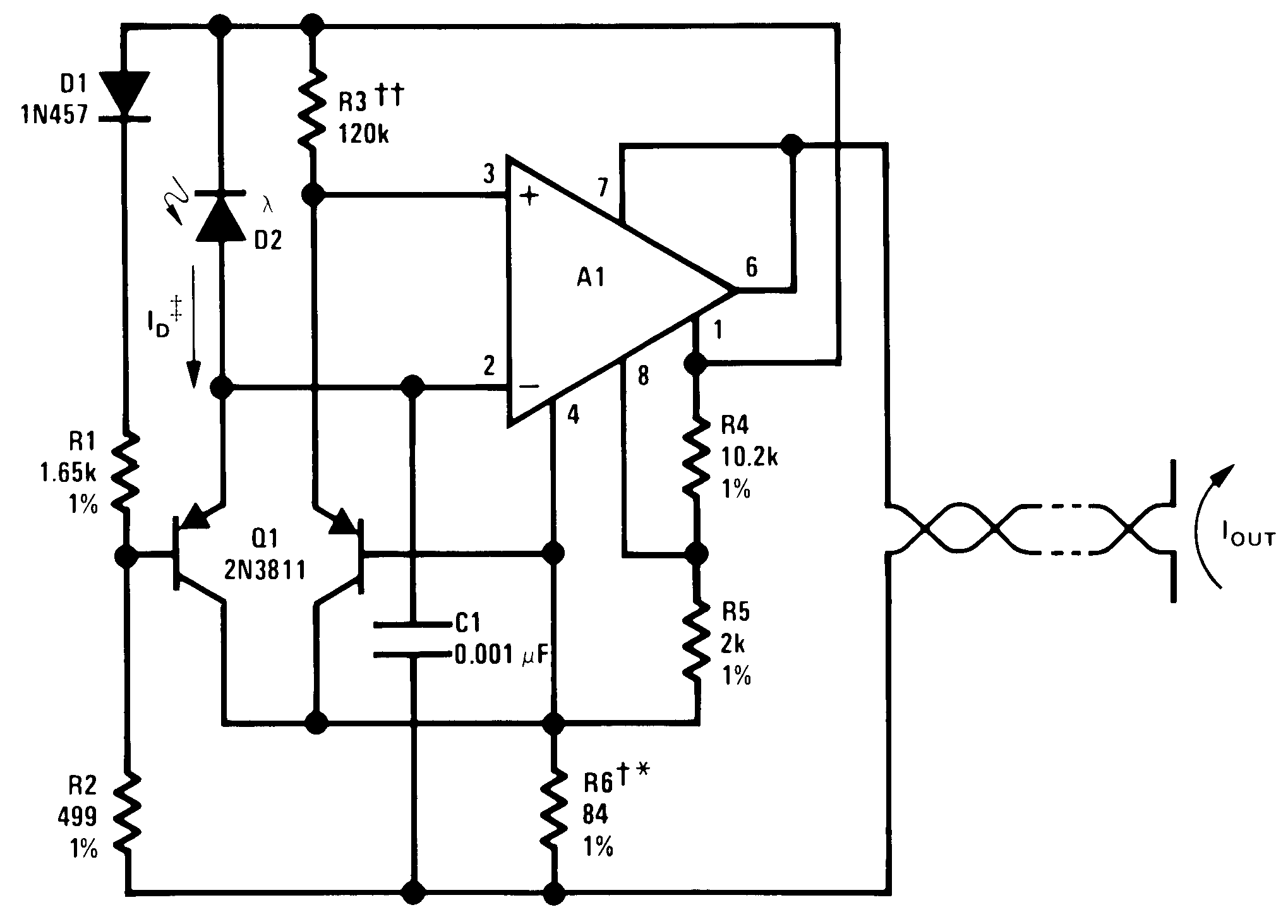
‡50 μA≤ID≤500 μA
††Center Scale Trim
†Scale Factor Trim
*Copper Wire Wound
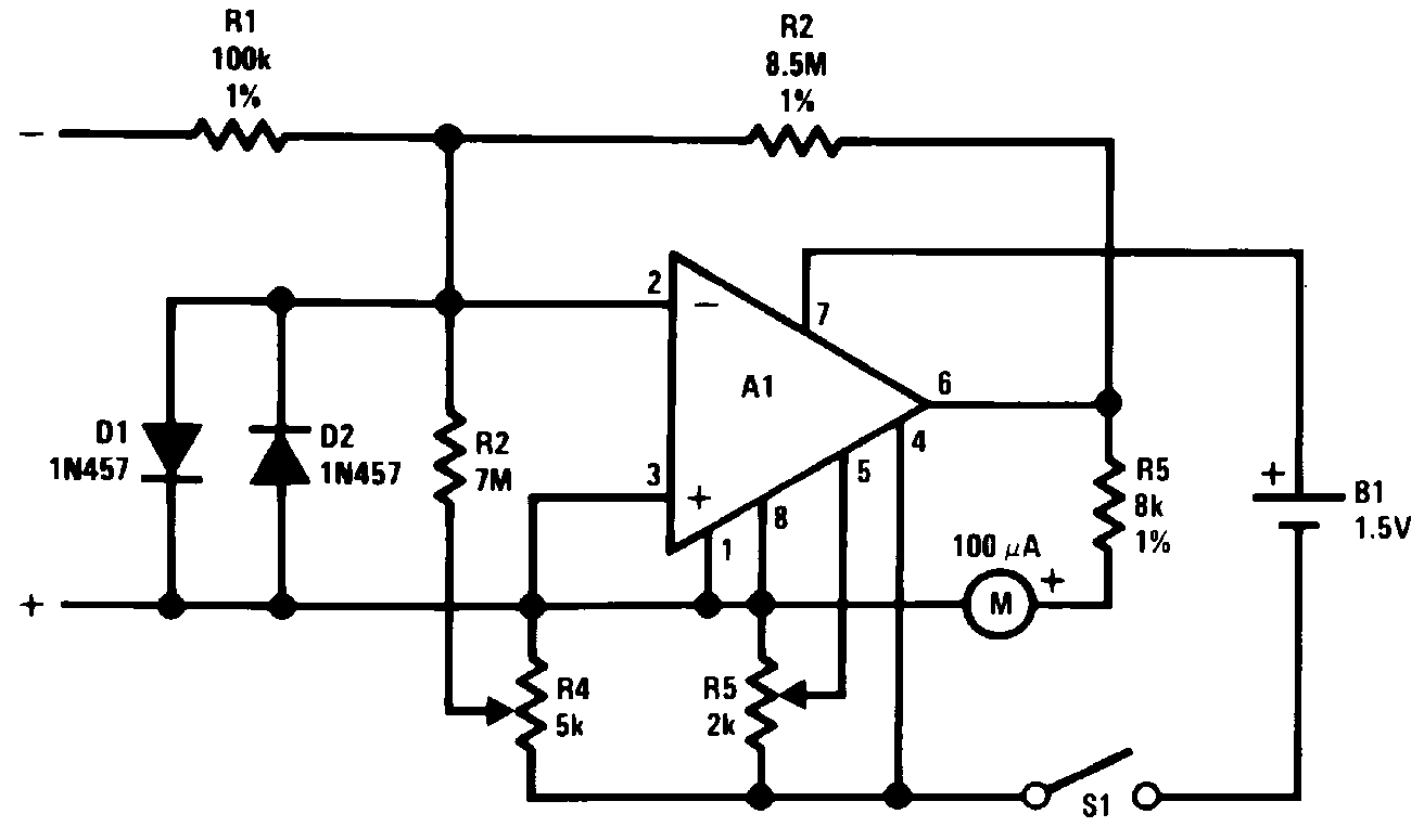
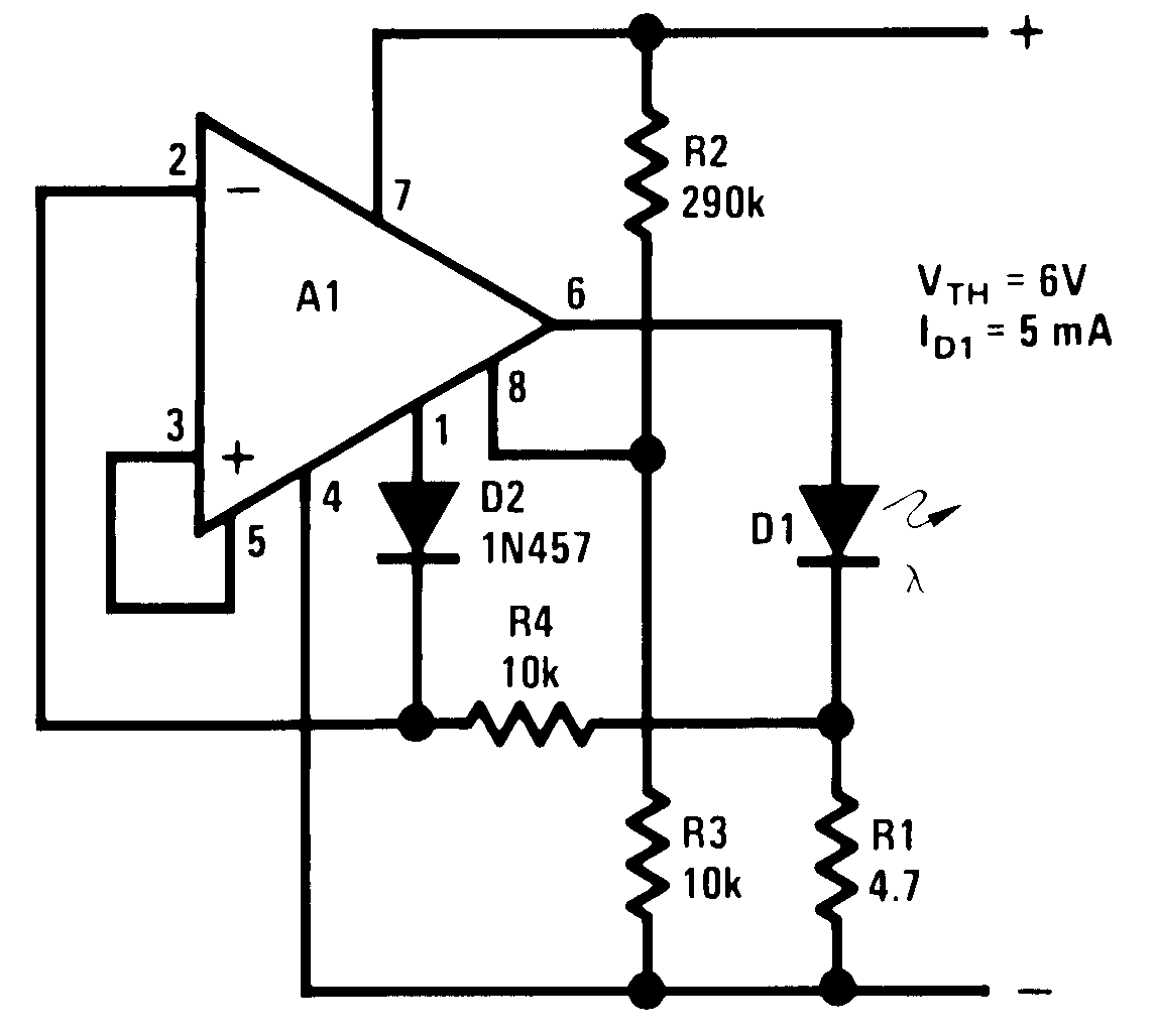 Figure 62. Battery-threshold Indicator
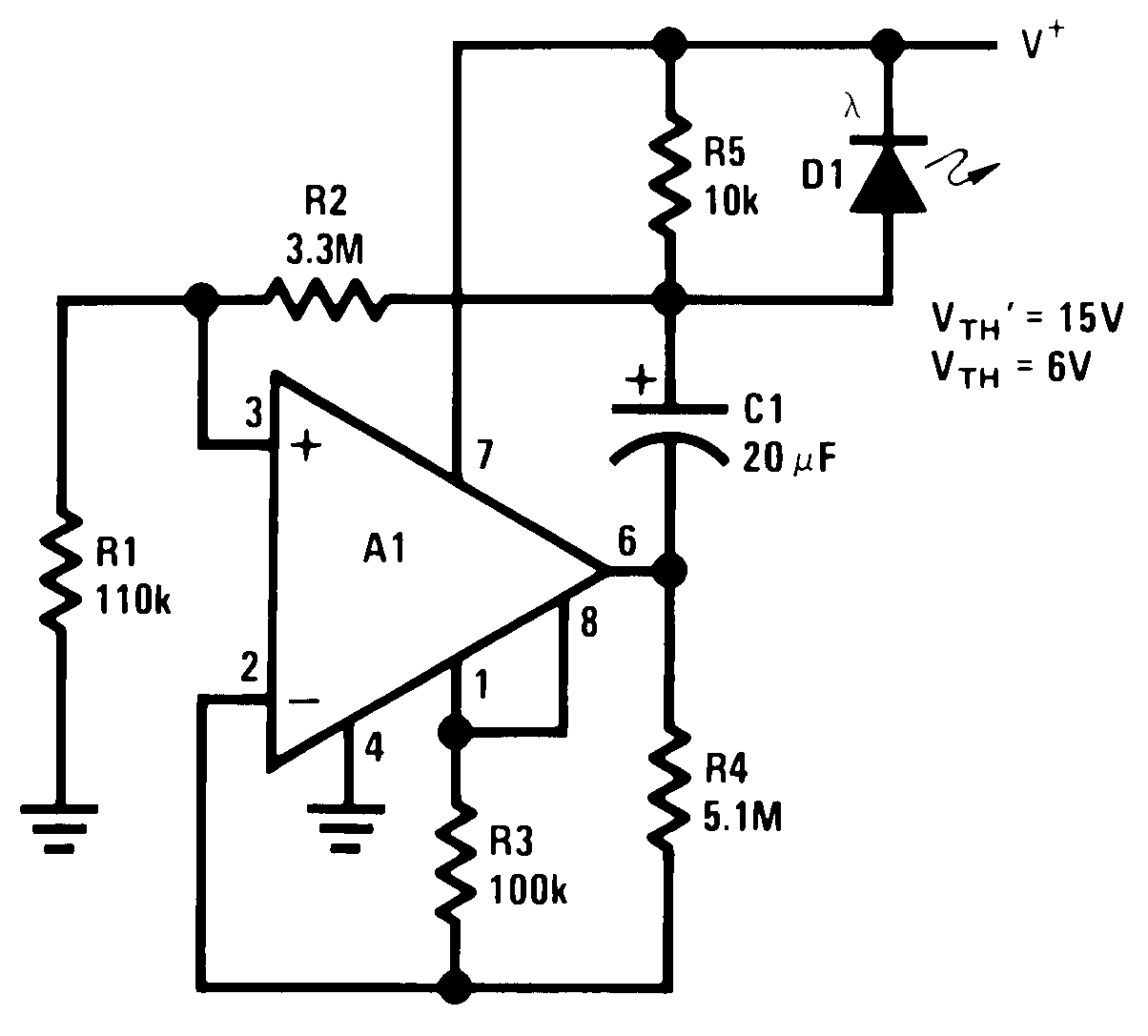
Above 6V and Below 15V
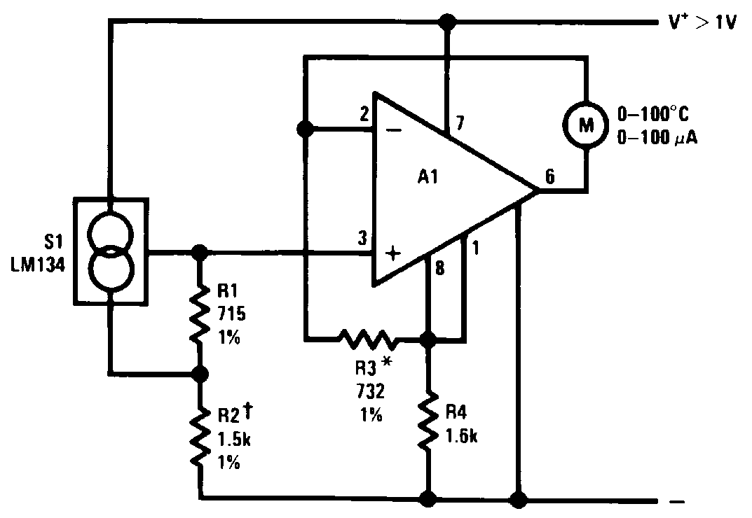
†Trim For Zero
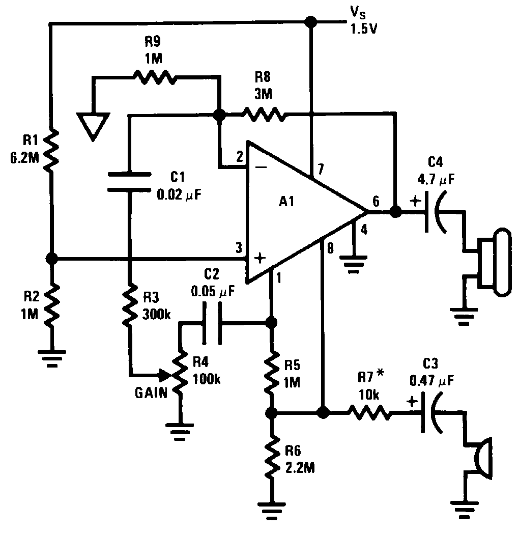
AV≤1k
f1∼100 Hz
f2∼5 kHz
RL∼500
*Max Gain Trim
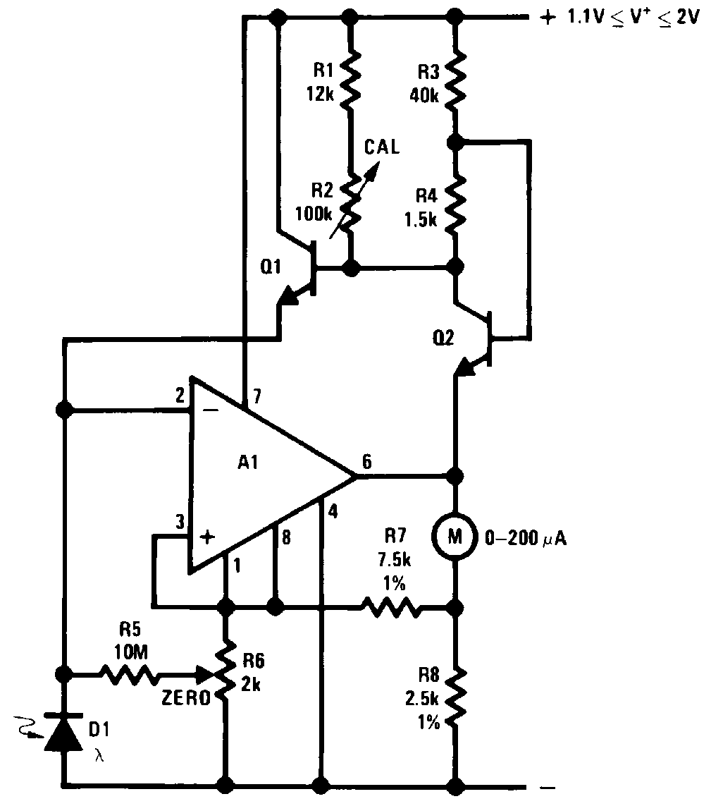
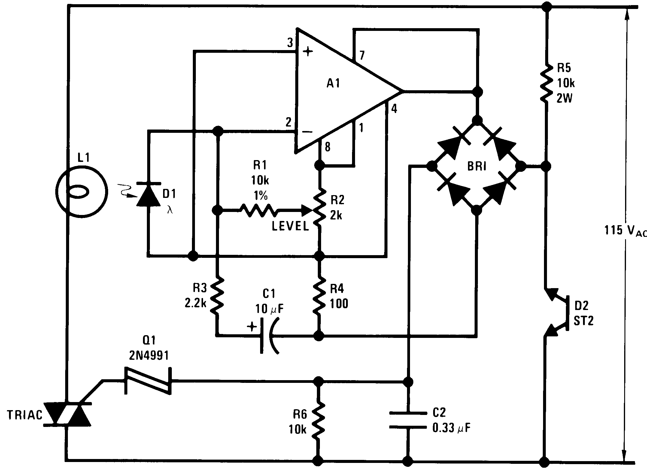 Figure 70. Light-Level Controller
8.3.3 Reference and Internal Regulator
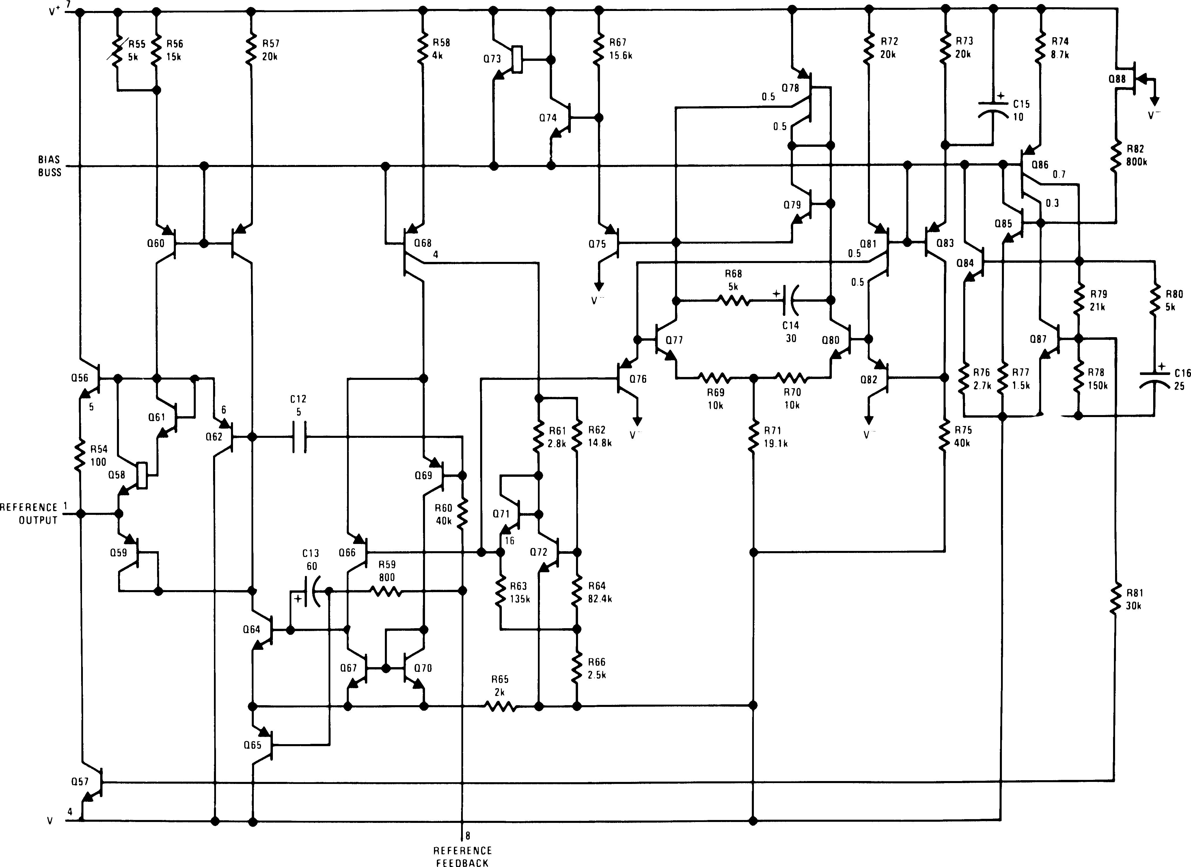 Figure 71. Reference and Internal Regulator