SNVS714F April 2011 – August 2015 LM25117 , LM25117-Q1
PRODUCTION DATA.
- 1 Features
- 2 Applications
- 3 Description
- 4 Revision History
- 5 Pin Configuration and Functions
- 6 Specifications
-
7 Detailed Description
- 7.1 Overview
- 7.2 Functional Block Diagram
- 7.3
Feature Description
- 7.3.1 High Voltage Startup Regulator and VCC Disable
- 7.3.2 UVLO
- 7.3.3 Oscillator And Sync Capability
- 7.3.4 Ramp Generator and Emulated Current Sense
- 7.3.5 Error Amplifier and PWM Comparator
- 7.3.6 Soft-Start
- 7.3.7 Cycle-By-Cycle Current Limit
- 7.3.8 Hiccup Mode Current Limiting
- 7.3.9 HO and LO Drivers
- 7.3.10 Current Monitor
- 7.3.11 Maximum Duty Cycle
- 7.3.12 Thermal Protection
- 7.4 Device Functional Modes
-
8 Application and Implementation
- 8.1 Application Information
- 8.2 Typical Applications
- 8.3
Detailed Design Procedure
- 8.3.1 Feedback Compensation
- 8.3.2 Sub-Harmonic Oscillation
- 8.3.3 Design Requirements
- 8.3.4 Timing Resistor RT
- 8.3.5 Output Inductor LO
- 8.3.6 Diode Emulation Function
- 8.3.7 Current Sense Resistor RS
- 8.3.8 Current Sense Filter RCS and CCS
- 8.3.9 Ramp Resistor RRAMP and Ramp Capacitor CRAMP
- 8.3.10 UVLO Divider RUV2, RUV1 and CFT
- 8.3.11 VCC Disable and External VCC Supply
- 8.3.12 Power Switches QH and QL
- 8.3.13 Snubber Components RSNB and CSNB
- 8.3.14 Bootstrap Capacitor CHB and Bootstrap Diode DHB
- 8.3.15 VCC Capacitor CVCC
- 8.3.16 Output Capacitor CO
- 8.3.17 Input Capacitor CIN
- 8.3.18 VIN Filter RVIN, CVIN
- 8.3.19 Soft-Start Capacitor CSS
- 8.3.20 Restart Capacitor CRES
- 8.3.21 Output Voltage Divider RFB2 and RFB1
- 8.3.22 Loop Compensation Components CCOMP, RCOMP and CHF
- 8.4 Application Curves
- 9 Power Supply Recommendations
- 10Layout
- 11Device and Documentation Support
- 12Mechanical, Packaging, and Orderable Information
Package Options
Mechanical Data (Package|Pins)
Thermal pad, mechanical data (Package|Pins)
Orderable Information
10 Layout
10.1 Layout Guideline
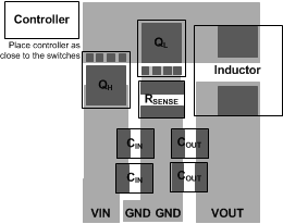
 Figure 38. Layout Example
10.1.1 PC Board Layout Recommendations
In a buck regulator the primary switching loop consists of the input capacitor, NMOS power switches and current sense resistor. Minimizing the area of this loop reduces the stray inductance and minimizes noise and possible erratic operation. High quality input capacitors should be placed as close as possible to the NMOS power switches, with the VIN side of the capacitor connected directly to the high-side NMOS drain and the ground side of the capacitor connected as close as possible to the current sense resistor ground connection.
Connect all of the low power ground connections (RUV1, RT, RFB1, CSS, CRES, CCM, CVIN, CRAMP) directly to the regulator AGND pin. Connect CVCC directly to the regulator PGND pin. Note that CVIN and CVCC must be as physically close as possible to the IC. AGND and PGND must be directly connected together through a top-side copper pattern connected to the exposed pad. Ensure no high current flows beneath the underside exposed pad.
The LM25117 has an exposed thermal pad to aid power dissipation. Adding several vias under the exposed pad helps conduct heat away from the IC. The junction to ambient thermal resistance varies with application. The most significant variables are the area of copper in the PC board, the number of vias under the exposed pad and the amount of forced air cooling. The integrity of the solder connection from the IC exposed pad to the PC board is critical. Excessive voids greatly decrease the thermal dissipation capacity.
The highest power dissipating components are the two power switches. Selecting NMOS switches with exposed pads aids the power dissipation of these devices.