SNVS123D April 1998 – May 2016 LM2599
PRODUCTION DATA.
- 1 Features
- 2 Applications
- 3 Description
- 4 Revision History
- 5 Description (continued)
- 6 Pin Configuration and Functions
-
7 Specifications
- 7.1 Absolute Maximum Ratings
- 7.2 ESD Ratings
- 7.3 Recommended Operating Conditions
- 7.4 Thermal Information
- 7.5 Electrical Characteristics - 3.3-V Version
- 7.6 Electrical Characteristics - 5-V Version
- 7.7 Electrical Characteristics - 12-V Version
- 7.8 Electrical Characteristics - Adjustable Voltage Version
- 7.9 Electrical Characteristics - All Output Voltage Versions
- 7.10 Typical Characteristics
- 8 Detailed Description
-
9 Application and Implementation
- 9.1
Application Information
- 9.1.1 Soft-Start Capacitor (CSS)
- 9.1.2 Delay Capacitor (CDELAY)
- 9.1.3 Feedforward Capacitor (CFF) for Adjustable Output Voltage Version Only
- 9.1.4 Input Capacitor (CIN)
- 9.1.5 Output Capacitor (COUT)
- 9.1.6 Catch Diode
- 9.1.7 Inductor Selection
- 9.1.8 Output Voltage Ripple and Transients
- 9.1.9 Open Core Inductors
- 9.2 Typical Applications
- 9.1
Application Information
- 10Power Supply Recommendations
- 11Layout
- 12Device and Documentation Support
- 13Mechanical, Packaging, and Orderable Information
Package Options
Mechanical Data (Package|Pins)
Thermal pad, mechanical data (Package|Pins)
- KTW|7
Orderable Information
6 Pin Configuration and Functions
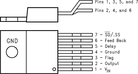
NDZ Package
7-Pin TO-220
Top View

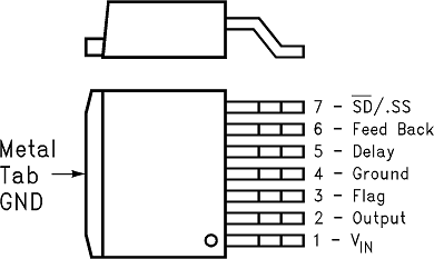
KTW Package
7-Pin TO-263
Top View

Pin Functions(1)
| PIN | I/O | DESCRIPTION | |
|---|---|---|---|
| NO. | NAME | ||
| 1 | +VIN | I | This is the positive input supply for the IC switching regulator. A suitable input bypass capacitor must be present at this pin to minimize voltage transients and to supply the switching currents needed by the regulator. |
| 2 | Output | O | Internal switch. The voltage at this pin switches between approximately (+VIN − VSAT) and approximately −0.5 V, with a duty cycle of VOUT/VIN. To minimize coupling to sensitive circuitry, the PCB copper area connected to this pin must be kept to a minimum. |
| 3 | Error Flag | O | Open-collector output that provides a low signal (flag transistor ON) when the regulated output voltage drops more than 5% from the nominal output voltage. On start up, Error Flag is low until VOUT reaches 95% of the nominal output voltage and a delay time determined by the Delay pin capacitor. This signal can be used as a reset to a microprocessor on power-up. |
| 4 | Ground | — | Circuit ground. |
| 5 | Delay | O | At power-up, this pin can be used to provide a time delay between the time the regulated output voltage reaches 95% of the nominal output voltage, and the time the error flag output goes high. |
| 6 | Feedback | I | Senses the regulated output voltage to complete the feedback loop. |
| 7 | Shutdown/Soft-start | I | This dual function pin provides the following features: (a) Allows the switching regulator circuit to be shut down using logic level signals thus dropping the total input supply current to approximately 80 μA. (b) Adding a capacitor to this pin provides a soft-start feature which minimizes start-up current and provides a controlled ramp up of the output voltage. |
(1) If any of the above three features (Shutdown/Soft-start, Error Flag, or Delay) are not used, the respective pins must be left open.