SNVS033D May   2004  – November 2015 LM2621

PRODUCTION DATA.  

  1. Features
  2. Applications
  3. Description
  4. Revision History
  5. Pin Configuration and Functions
  6. Specifications
    1. 6.1 Absolute Maximum Ratings
    2. 6.2 Recommended Operating Conditions
    3. 6.3 Thermal Information
    4. 6.4 Electrical Characteristics
    5. 6.5 Typical Characteristics
  7. Detailed Description
    1. 7.1 Overview
    2. 7.2 Functional Block Diagram
    3. 7.3 Feature Description
      1. 7.3.1 Gated Oscillator Control Scheme
      2. 7.3.2 Low Voltage Start-Up
      3. 7.3.3 Output Voltage Ripple Frequency
      4. 7.3.4 Internal Current Limit and Thermal Protection
    4. 7.4 Device Functional Modes
      1. 7.4.1 Shutdown
  8. Application and Implementation
    1. 8.1 Application Information
    2. 8.2 Typical Applications
      1. 8.2.1 Step-Up DC-DC Converter Typical Application Using LM2621
        1. 8.2.1.1 Design Requirements
        2. 8.2.1.2 Detailed Design Procedure
          1. 8.2.1.2.1 Setting the Output Voltage
          2. 8.2.1.2.2 Bootstrapping
          3. 8.2.1.2.3 Setting the Switching Frequency
          4. 8.2.1.2.4 Inductor Selection
          5. 8.2.1.2.5 Output Diode Selection
          6. 8.2.1.2.6 Input and Output Filter Capacitors Selection
        3. 8.2.1.3 Application Curves
      2. 8.2.2 5-V / 0.5-A Step-Up Regulator
        1. 8.2.2.1 Design Requirements
        2. 8.2.2.2 Detailed Design Procedure
      3. 8.2.3 2-mm Tall 5-V / 0.2-A Step-Up Regulator for Low Profile Applications
        1. 8.2.3.1 Design Requirements
        2. 8.2.3.2 Detailed Design Procedure
      4. 8.2.4 3.3-V / 0.5-A SEPIC Regulator
        1. 8.2.4.1 Design Requirements
        2. 8.2.4.2 Detailed Design Procedure
  9. Power Supply Recommendations
  10. 10Layout
    1. 10.1 Layout Guidelines
    2. 10.2 Layout Example
  11. 11Device and Documentation Support
    1. 11.1 Device Support
      1. 11.1.1 Third-Party Products Disclaimer
    2. 11.2 Documentation Support
      1. 11.2.1 Related Documentation
    3. 11.3 Community Resources
    4. 11.4 Trademarks
    5. 11.5 Electrostatic Discharge Caution
    6. 11.6 Glossary
  12. 12Mechanical, Packaging, and Orderable Information

Package Options

Mechanical Data (Package|Pins)
Thermal pad, mechanical data (Package|Pins)
Orderable Information

5 Pin Configuration and Functions

DGK Package
8-Pin VSSOP
Top View
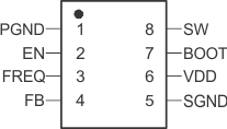
LM2621 10093418.gif

Pin Functions

PIN TYPE(1) DESCRIPTION
NAME NO.
PGND 1 GND Power Ground
EN 2 I Active-Low Shutdown Input
FREQ 3 A Frequency Adjust. An external resistor connected between this pin and Pin 6 (VDD) sets the switching frequency of the LM2621.
FB 4 A Output Voltage Feedback
SGND 5 GND Signal Ground
VDD 6 PWR Power Supply for Internal Circuitry
BOOT 7 PWR Bootstrap Supply for the Gate Drive of Internal MOSFET Power Switch
SW 8 PWR Drain of the Internal MOSFET Power Switch
(1) I = Input, O = Output, PWR = Power, GND = Ground, A = Analog