SNVS487E December 2006 – January 2015 LM27313 , LM27313-Q1
PRODUCTION DATA.
- 1 Features
- 2 Applications
- 3 Description
- 4 Revision History
- 5 Pin Configuration and Functions
- 6 Specifications
- 7 Detailed Description
-
8 Application and Implementation
- 8.1 Application Information
- 8.2
Typical Applications
- 8.2.1
Application Circuit VIN=5.0 V, VOUT=12.0 V, Iload=250 mA
- 8.2.1.1 Design Requirements
- 8.2.1.2
Detailed Design Procedure
- 8.2.1.2.1 Selecting the External Capacitors
- 8.2.1.2.2 Selecting the Output Capacitor
- 8.2.1.2.3 Selecting the Input Capacitor
- 8.2.1.2.4 Feed-Forward Compensation
- 8.2.1.2.5 Selecting Diodes
- 8.2.1.2.6 Setting the Output Voltage
- 8.2.1.2.7 Duty Cycle
- 8.2.1.2.8 Inductance Value
- 8.2.1.2.9 Maximum Switch Current
- 8.2.1.2.10 Calculating Load Current
- 8.2.1.2.11 Design Parameters VSW and ISW
- 8.2.1.2.12 Minimum Inductance
- 8.2.1.2.13 Inductor Suppliers
- 8.2.1.2.14 Shutdown Pin Operation
- 8.2.1.3 Application Curves
- 8.2.2 Application Circuit VIN=5.0V, VOUT=20.0V, Iload=150mA
- 8.2.1
Application Circuit VIN=5.0 V, VOUT=12.0 V, Iload=250 mA
- 9 Power Supply Recommendations
- 10Layout
- 11Device and Documentation Support
- 12Mechanical, Packaging, and Orderable Information
Package Options
Mechanical Data (Package|Pins)
- DBV|5
Thermal pad, mechanical data (Package|Pins)
Orderable Information
8 Application and Implementation
NOTE
Information in the following applications sections is not part of the TI component specification, and TI does not warrant its accuracy or completeness. TI’s customers are responsible for determining suitability of components for their purposes. Customers should validate and test their design implementation to confirm system functionality.
8.1 Application Information
The device operates with input voltage in the range of 2.7 V to 14 V and provides regulated output voltage. This device is optimized for high-efficiency operation with minimum number of external components. Also, high switching frequency allows use of small surface mount components, enabling very small solution size. For component selection, refer to Detailed Design Procedure.
8.2 Typical Applications
8.2.1 Application Circuit VIN=5.0 V, VOUT=12.0 V, Iload=250 mA
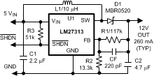 Figure 12. Typical Application Circuit
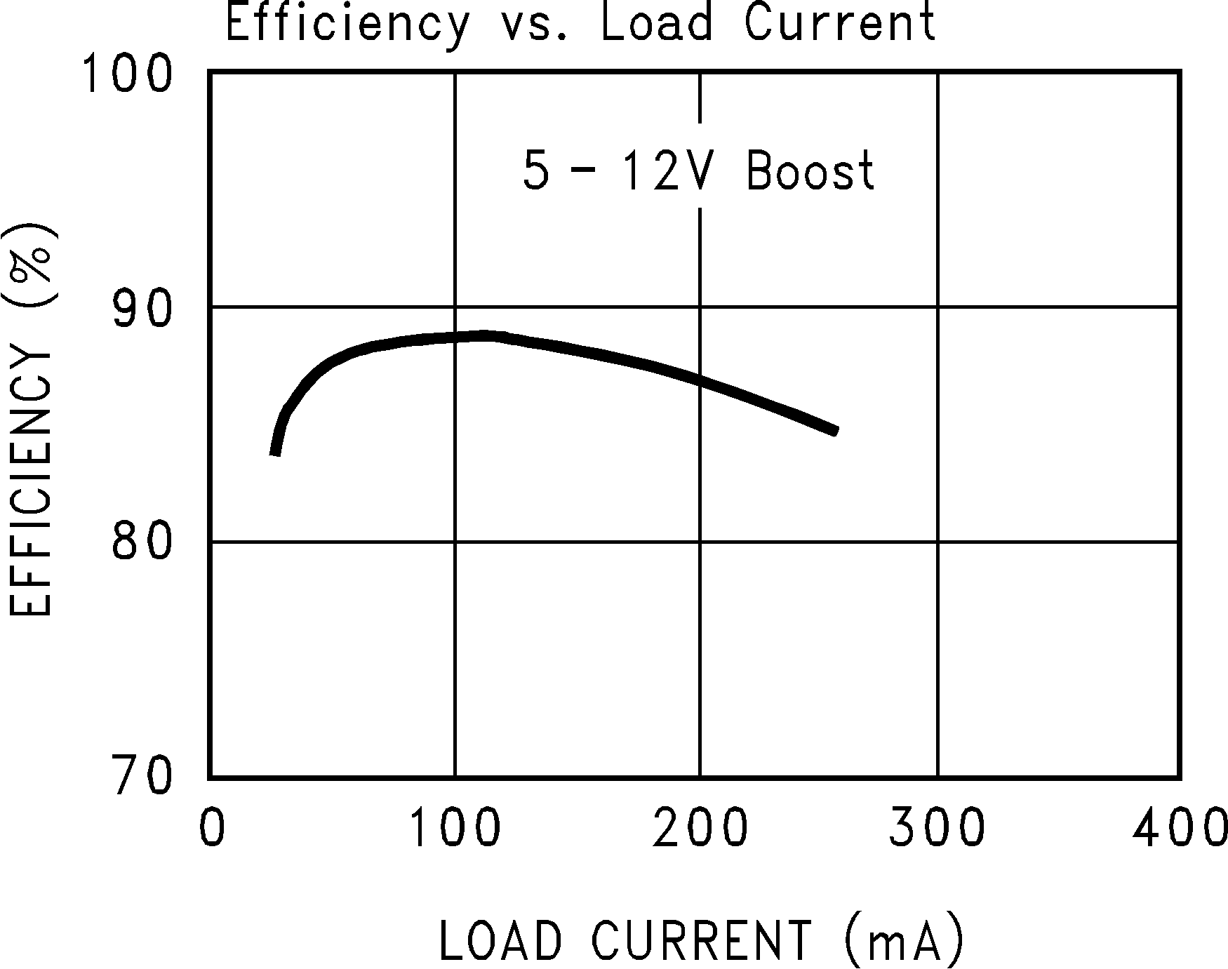 Figure 13. Efficiency vs. Load Current
8.2.1.1 Design Requirements
The device must be able to operate at any voltage within input voltage range.
Load Current must be defined in order to properly size the inductor, input and output capacitors. The inductor should be able to handle full expected load current as well as the peak current generated during load transients and start up. Inrush current at startup will depend on the output capacitor selection. More details are provided in Detailed Design Procedure.
Device has a shutdown pin (SHDN) that is used to enable and disable device. This pin is active low and should be tied to VIN if not used in application.
8.2.1.2 Detailed Design Procedure
8.2.1.2.1 Selecting the External Capacitors
The LM27313 requires ceramic capacitors at the input and output to accommodate the peak switching currents the part needs to operate. Electrolytic capacitors have resonant frequencies which are below the switching frequency of the device, and therefore can not provide the currents needed to operate. Electrolytics may be used in parallel with the ceramics for bulk charge storage which will improve transient response.
When selecting a ceramic capacitor, only X5R and X7R dielectric types should be used. Other types such as Z5U and Y5F have such severe loss of capacitance due to effects of temperature variation and applied voltage, they may provide as little as 20% of rated capacitance in many typical applications. Always consult capacitor manufacturer’s data curves before selecting a capacitor. High-quality ceramic capacitors can be obtained from Taiyo-Yuden, AVX, and Murata.
8.2.1.2.2 Selecting the Output Capacitor
A single ceramic capacitor of value 4.7 µF to 10 µF provides sufficient output capacitance for most applications. For output voltages below 10 V, a 10 µF capacitance is required. If larger amounts of capacitance are desired for improved line support and transient response, tantalum capacitors can be used in parallel with the ceramics. Aluminum electrolytics with ultra low ESR such as Sanyo Oscon can be used, but are usually prohibitively expensive. Typical AI electrolytic capacitors are not suitable for switching frequencies above
500 kHz due to significant ringing and temperature rise due to self-heating from ripple current. An output capacitor with excessive ESR can also reduce phase margin and cause instability.
8.2.1.2.3 Selecting the Input Capacitor
An input capacitor is required to serve as an energy reservoir for the current which must flow into the inductor each time the switch turns ON. This capacitor must have extremely low ESR and ESL, so ceramic must be used. We recommend a nominal value of 2.2 µF, but larger values can be used. Because this capacitor reduces the amount of voltage ripple seen at the input pin, it also reduces the amount of EMI passed back along that line to other circuitry.
8.2.1.2.4 Feed-Forward Compensation
Although internally compensated, the feed-forward capacitor Cf is required for stability (see Equation 1). Adding this capacitor puts a zero in the loop response of the converter. Without it, the regulator loop can oscillate. The recommended frequency for the zero fz should be approximately 8 kHz. Cf can be calculated using the formula:
8.2.1.2.5 Selecting Diodes
The external diode used in the typical application should be a Schottky diode. If the switch voltage is less than 15V, a 20V diode such as the MBR0520 is recommended. If the switch voltage is between 15 V and 25 V, a 30-V diode such as the MBR0530 is recommended. If the switch voltage exceeds 25V, a 40V diode such as the MBR0540 should be used.
The MBR05xx series of diodes are designed to handle a maximum average current of 500 mA. For applications with load currents to 800 mA, a Microsemi UPS5817 can be used.
8.2.1.2.6 Setting the Output Voltage
The output voltage is set using the external resistors R1 and R2 (see Equation 2). A value of 13.3 kΩ is recommended for R2 to establish a divider current of approximately 92 µA. R1 is calculated using the formula:
8.2.1.2.7 Duty Cycle
The maximum duty cycle of the switching regulator determines the maximum boost ratio of output-to-input voltage that the converter can attain in continuous mode of operation. The duty cycle for a given boost application is defined as:
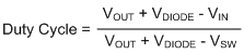
This applies for continuous mode operation.
The equation shown for calculating duty cycle incorporates terms for the FET switch voltage and diode forward voltage. The actual duty cycle measured in operation will also be affected slightly by other power losses in the circuit such as wire losses in the inductor, switching losses, and capacitor ripple current losses from self-heating. Therefore, the actual (effective) duty cycle measured may be slightly higher than calculated to compensate for these power losses. A good approximation for effective duty cycle is:
where
- the efficiency can be approximated from the curves provided.
8.2.1.2.8 Inductance Value
The first question we are usually asked is: “How small can I make the inductor?” (because they are the largest sized component and usually the most costly). The answer is not simple and involves trade-offs in performance. More inductance means less inductor ripple current and less output voltage ripple (for a given size of output capacitor). More inductance also means more load power can be delivered because the energy stored during each switching cycle is:
where
- lp is the peak inductor current.
An important point to observe is that the LM27313 will limit its switch current based on peak current. This means that because lp(max) is fixed, increasing L will increase the maximum amount of power available to the load. Conversely, using too little inductance may limit the amount of load current which can be drawn from the output.
Best performance is usually obtained when the converter is operated in “continuous” mode at the load current range of interest, typically giving better load regulation and less output ripple. Continuous operation is defined as not allowing the inductor current to drop to zero during the cycle. It should be noted that all boost converters shift over to discontinuous operation as the output load is reduced far enough, but a larger inductor stays “continuous” over a wider load current range.
To better understand these tradeoffs, a typical application circuit (5V to 12V boost with a 10 µH inductor) will be analyzed.
Because the LM27313 typical switching frequency is 1.6 MHz, the typical period is equal to 1/fSW(TYP), or approximately 0.625 µs.
We will assume: VIN = 5 V, VOUT = 12 V, VDIODE = 0.5 V, VSW = 0.5 V. The duty cycle is:
The typical ON time of the switch is:
It should be noted that when the switch is ON, the voltage across the inductor is approximately 4.5 V.
Use the equation:
Then, calculate the di/dt rate of the inductor which is found to be 0.45 A/µs during the ON time. Using these facts, we can then show what the inductor current will look like during operation:
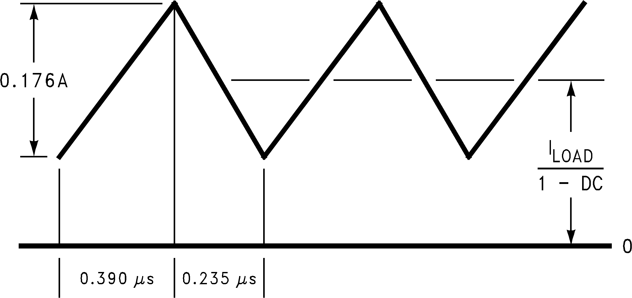 Figure 14. 10 µH Inductor Current, 5 V – 12 V Boost
During the 0.390-µs ON time, the inductor current ramps up 0.176 A and ramps down an equal amount during the OFF time. This is defined as the inductor “ripple current”. It can also be seen that if the load current drops to about 33 mA, the inductor current will begin touching the zero axis which means it will be in discontinuous mode. A similar analysis can be performed on any boost converter, to make sure the ripple current is reasonable and continuous operation will be maintained at the typical load current values.
8.2.1.2.9 Maximum Switch Current
The maximum FET switch current available before the current limiter cuts in is dependent on duty cycle of the application. This is illustrated in Figure 15 which shows typical values of switch current as a function of effective (actual) duty cycle:
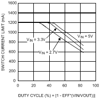 Figure 15. Switch Current Limit vs Duty Cycle
8.2.1.2.10 Calculating Load Current
As shown in Figure 14 which depicts inductor current, the load current is related to the average inductor current by the relation:
where
- DC is the duty cycle of the application.
The switch current can be found by:
Inductor ripple current is dependent on inductance, duty cycle, input voltage and frequency:
Combining all terms, we can develop an expression which allows the maximum available load current to be calculated:
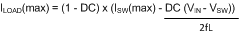
The equation shown to calculate maximum load current takes into account the losses in the inductor or turn-OFF switching losses of the FET and diode. For actual load current in typical applications, we took bench data for various input and output voltages and displayed the maximum load current available for a typical device in graph form:
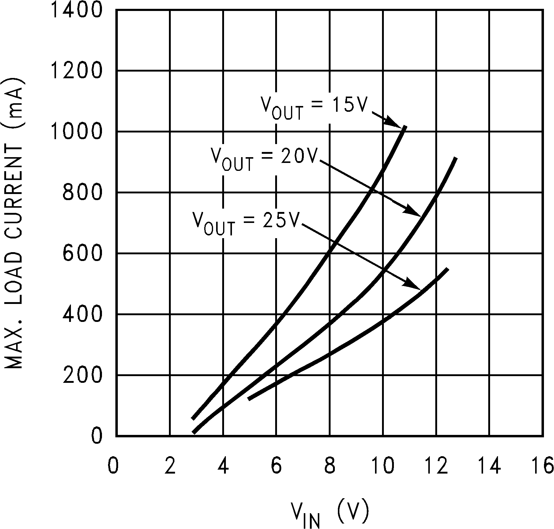 Figure 16. Max. Load Current vs VIN
8.2.1.2.11 Design Parameters VSW and ISW
The value of the FET ON voltage (referred to as VSW in the equations) is dependent on load current. A good approximation can be obtained by multiplying the "ON Resistance" of the FET times the average inductor current.
FET ON resistance increases at VIN values below 5V, because the internal N-FET has less gate voltage in this input voltage range (see Typical Characteristics). Above VIN = 5 V, the FET gate voltage is internally clamped to 5V.
The maximum peak switch current the device can deliver is dependent on duty cycle. The minimum switch current value (ISW) is ensured to be at least 800 mA at duty cycles below 50%. For higher duty cycles, see Typical Characteristics.
8.2.1.2.12 Minimum Inductance
In some applications where the maximum load current is relatively small, it may be advantageous to use the smallest possible inductance value for cost and size savings. The converter will operate in discontinuous mode in such a case.
The minimum inductance should be selected such that the inductor (switch) current peak on each cycle does not reach the 800 mA current limit maximum. To understand how to do this, an example will be presented.
In this example, the LM27313 nominal switching frequency is 1.6 MHz, and the minimum switching frequency is 1.15 MHz. This means the maximum cycle period is the reciprocal of the minimum frequency:
Assume: VIN = 5 V, VOUT = 12 V, VSW = 0.2 V, and VDIODE = 0.3 V. The duty cycle is:
Therefore, the maximum switch ON time is:
An inductor should be selected with enough inductance to prevent the switch current from reaching 800 mA in the 0.524 µs ON time interval (see Figure 17):
 Figure 17. Discontinuous Design, 5 V – 12 V Boost
The voltage across the inductor during ON time is 4.8 V. Minimum inductance value is found by:
In this case, a 3.3-µH inductor could be used, assuming it provided at least that much inductance up to the 800-mA current value. This same analysis can be used to find the minimum inductance for any boost application.
8.2.1.2.13 Inductor Suppliers
Some of the recommended suppliers of inductors for this product include, but are not limited to, Sumida, Coilcraft, Panasonic, TDK and Murata. When selecting an inductor, make certain that the continuous current rating is high enough to avoid saturation at peak currents. A suitable core type must be used to minimize core (switching) losses, and wire power losses must be considered when selecting the current rating.
8.2.1.2.14 Shutdown Pin Operation
The device is turned off by pulling the shutdown pin low. If this function is not going to be used, the pin should be tied directly to VIN. If the SHDN function will be needed, a pullup resistor must be used to VIN (50 kΩ to 100 kΩ is recommended), or the pin must be actively driven high and low. The SHDN pin must not be left unterminated.
8.2.1.3 Application Curves
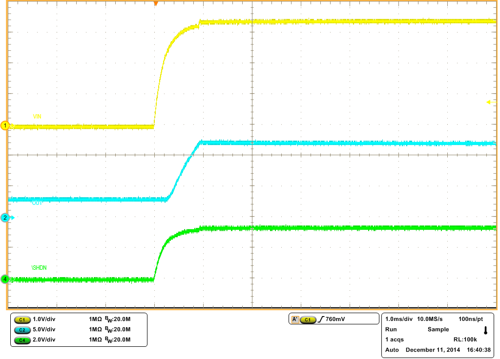 Figure 18. Typical Startup Waveform for Vin = 3.3 V, Vout = 12 V
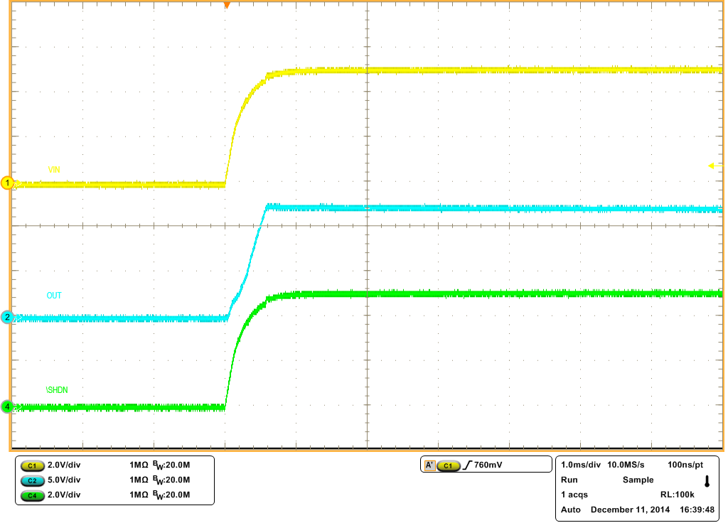 Figure 19. Typical Startup Waveform for Vin = 5.0 V, Vout = 12 V
8.2.2 Application Circuit VIN=5.0V, VOUT=20.0V, Iload=150mA
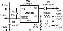 Figure 20. Typical Application Circuit
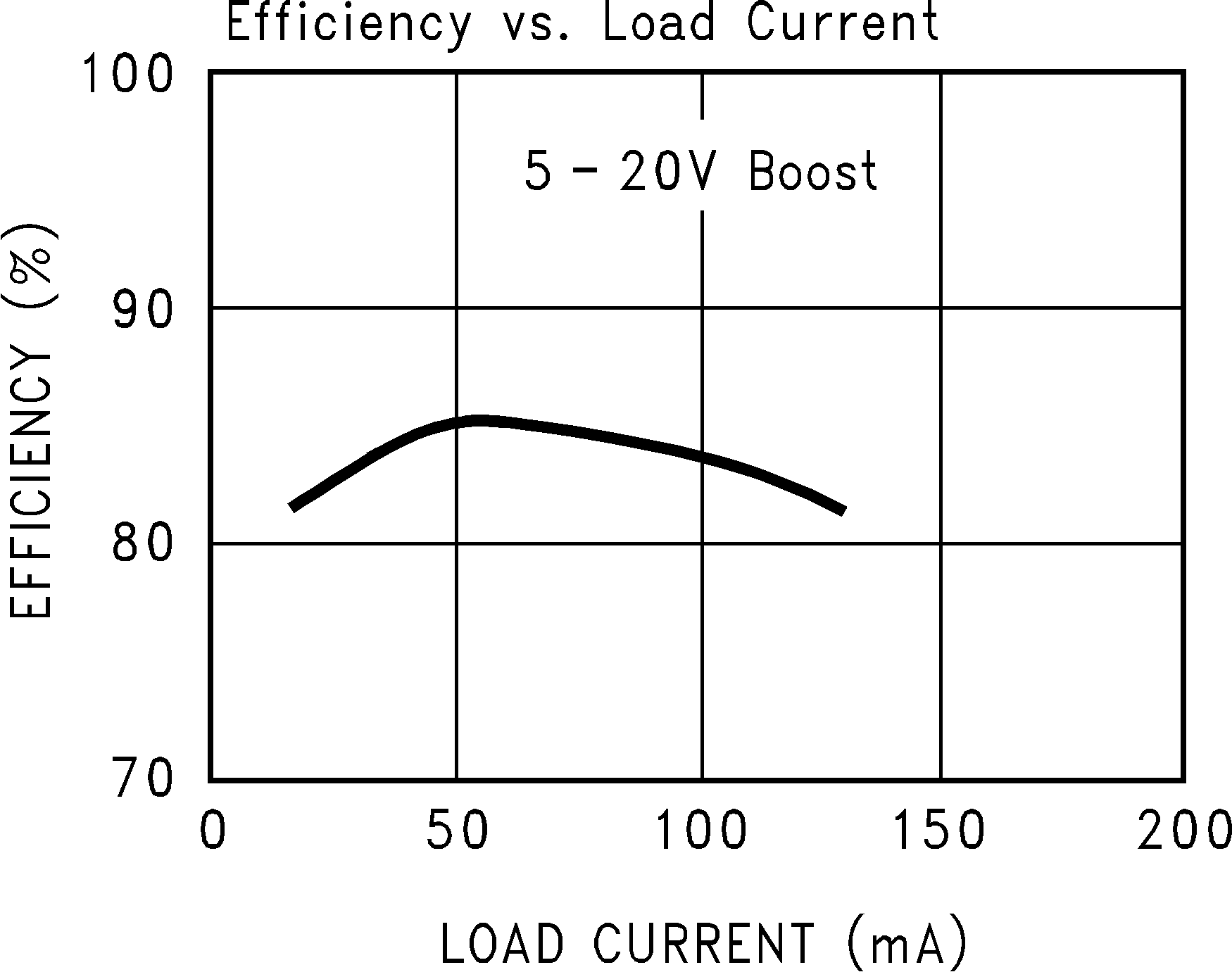 Figure 21. Efficiency vs. Load Current
8.2.2.1 Design Requirements
See Design Requirements.
8.2.2.2 Detailed Design Procedure
8.2.2.3 Application Curves
See Application Curves.