SNVS497F November 2008 – September 2016 LM27341 , LM27341-Q1 , LM27342 , LM27342-Q1
PRODUCTION DATA.
- 1 Features
- 2 Applications
- 3 Description
- 4 Revision History
- 5 Pin Configuration and Functions
- 6 Specifications
- 7 Detailed Description
-
8 Application and Implementation
- 8.1
Application Information
- 8.1.1 Inductor Selection
- 8.1.2 Inductor Material Selection
- 8.1.3 Input Capacitor
- 8.1.4 Output Capacitor
- 8.1.5 Catch Diode
- 8.1.6 Boost Diode (Optional)
- 8.1.7 Boost Capacitor
- 8.1.8 Output Voltage
- 8.1.9 Feedforward Capacitor (Optional)
- 8.1.10
Calculating Efficiency and Junction Temperature
- 8.1.10.1 Schottky Diode Conduction Losses
- 8.1.10.2 Inductor Conduction Losses
- 8.1.10.3 MOSFET Conduction Losses
- 8.1.10.4 MOSFET Switching Losses
- 8.1.10.5 IC Quiescent Losses
- 8.1.10.6 MOSFET Driver Losses
- 8.1.10.7 Total Power Losses
- 8.1.10.8 Efficiency Calculation Example
- 8.1.10.9 Calculating Junction Temperature
- 8.2
Typical Applications
- 8.2.1 LM2734x Configuration From VIN = 7 V to 16 V, VOUT = 5 V For Full Load at 2 MHz
- 8.2.2 LM2734x Configuration From VIN = 7 V to 16 V, VOUT = 5 V For Full Load at 1 MHz
- 8.2.3 LM2734x Configuration From VIN = 5 V to 16 V, VOUT = 3.3 V For Full Load at 2 MHz
- 8.2.4 LM2734x Configuration From VIN = 5 V to 16 V, VOUT = 3.3 V For Full Load at 2 MHz With SYNC = GND
- 8.2.5 LM2734x Configuration From VIN = 5 V to 16 V, VOUT = 3.3 V For Full Load at 2 MHz With SYNC = 1 MHz
- 8.2.6 LM2734x Configuration From VIN = 3.3 V to 16 V, VOUT = 1.8 V For Full Load at 2 MHz With SYNC = 1 GND
- 8.2.7 LM2734x Configuration From VIN = 3.3 V to 16 V, VOUT = 1.8 V For Full Load at 2 MHz With SYNC = 1 MHz
- 8.2.8 LM2734x Configuration From VIN = 3.3 V to 9 V, VOUT = 1.2 V For Full Load at 2 MHz With SYNC = 2 MHz
- 8.1
Application Information
- 9 Power Supply Recommendations
- 10Layout
- 11Device and Documentation Support
- 12Mechanical, Packaging, and Orderable Information
Package Options
Mechanical Data (Package|Pins)
Thermal pad, mechanical data (Package|Pins)
Orderable Information
7 Detailed Description
7.1 Overview
The LM2734x and LM2734x-Q1 are a constant-frequency, peak current-mode PWM buck regulator IC that delivers a 1.5-A or 2-A load current. The regulator has a preset switching frequency of 2 MHz. This high frequency allows the LM2734x and LM2734x-Q1 to operate with small surface-mount capacitors and inductors, resulting in a DC-DC converter that requires a minimum amount of board space. The LM2734x and LM2734x-Q1 are internally compensated, which reduces design time, and requires few external components.
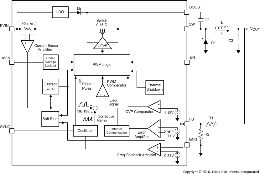
The following operating description of the LM2734x and LM2734x-Q1 refers to Functional Block Diagram and to the waveforms in Figure 27. The LM2734x and LM2734x-Q1 supply a regulated output voltage by switching the internal NMOS switch at a constant frequency and varying the duty cycle. A switching cycle begins at the falling edge of the reset pulse generated by the internal oscillator. When this pulse goes low, the output control logic turns on the internal NMOS switch. During this on-time, the SW pin voltage (VSW) swings up to approximately VIN, and the inductor current (iL) increases with a linear slope. The current-sense amplifier measures iL, which generates an output proportional to the switch current typically called the sense signal. The sense signal is summed with the regulator’s corrective ramp and compared to the error amplifier’s output, which is proportional to the difference between the feedback voltage (VFB) and VREF. When the output of the PWM comparator goes high, the switch turns off until the next switching cycle begins. During the switch off-time (tOFF), inductor current discharges through the catch diode D1, which forces the SW pin (VSW) to swing below ground by the forward voltage (VD1) of the catch diode. The regulator loop adjusts the duty cycle (D) to maintain a constant output voltage.
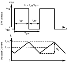 Figure 27. LM2734x Waveforms of SW Pin Voltage and Inductor Current
7.2 Functional Block Diagram
7.3 Feature Description
7.3.1 Boost Function
Capacitor C2 in Functional Block Diagram, commonly referred to as CBOOST, is used to store a voltage VBOOST. When LM2734x and LM2734x-Q1 start up, an internal LDO charges CBOOST through an internal diode, to a voltage sufficient to turn the internal NMOS switch on. The gate drive voltage supplied to the internal NMOS switch is VBOOST – VSW.
During a normal switching cycle, when the internal NMOS control switch is off (tOFF) (see Figure 27), VBOOST equals VLDO minus the forward voltage of the internal diode (VD2). At the same time the inductor current (iL) forward biases the catch diode D1 forcing the SW pin to swing below ground by the forward voltage drop of the catch diode (VD1). Therefore, the voltage stored across CBOOST is calculated with Equation 1 and Equation 2.
When the NMOS switch turns on (tON), the switch pin rises to Equation 3.
Then the D1 undergoes reverse biasing, and forces VBOOST to rise. The voltage at VBOOST is then calculated with Equation 4.
Which is approximately calculated with Equation 5.
VBOOST has pulled itself up by its bootstraps, or boosted to a higher voltage.
7.3.2 Low Input Voltage Considerations
When the input voltage is below 5 V and the duty cycle is greater than 75%, the gate drive voltage developed across CBOOST might not be sufficient for proper operation of the NMOS switch. In this case, CBOOST must be charged through an external Schottky diode attached to a 5-V voltage rail (see Figure 28). This ensures that the gate drive voltage is high enough for proper operation of the NMOS switch in the triode region. Maintain VBOOST – VSW less than the 6-V absolute maximum rating.
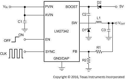 Figure 28. External Diode Charges CBOOST
7.3.3 High Output Voltage Considerations
When the output voltage is greater than 3.3 V, a minimum load current is required to charge CBOOST (see Figure 29). The minimum load current forward biases the catch diode D1 forcing the SW pin to swing below ground. This allows CBOOST to charge, ensuring that the gate drive voltage is high enough for proper operation. The minimum load current depends on many factors including the inductor value.
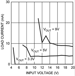 Figure 29. Minimum Load Current for L = 1.5 µH
7.3.4 Frequency Synchronization
The LM2734x and LM2734x-Q1 switching frequency can be synchronized to an external clock, between 1 MHz and 2.35 MHz, applied at the SYNC pin. At the first rising edge applied to the SYNC pin, the internal oscillator is overridden and subsequent positive edges initiate switching cycles. If the external SYNC signal is lost during operation, the LM2734x and LM2734x-Q1 revert to its internal 2-MHz oscillator within 1.5 µs. To disable frequency synchronization and use the internal 2-MHz oscillator, connect the SYNC pin to GND.
The SYNC pin gives the designer the flexibility to optimize their design. A lower switching frequency can be chosen for higher efficiency. A higher switching frequency can be chosen to keep EMI out of sensitive ranges such as the AM radio band. Synchronization can also be used to eliminate beat frequencies generated by the interaction of multiple switching power converters. Synchronizing multiple switching power converters result in cleaner power rails.
The selected switching frequency (fSYNC) and the minimum on-time (tMIN) limit the minimum duty cycle (DMIN) of the device as calculated with Equation 6.
Operation below DMIN is not recommended. The LM2734x and LM2734x-Q1 skip pulses to keep the output voltage in regulation, and the current limit is not ensured. The switching is in phase but no longer at the same switching frequency as the SYNC signal.
7.3.5 Current Limit
The LM2734x and LM2734x-Q1 use cycle-by-cycle current limiting to protect the output switch. During each switching cycle, a current limit comparator detects if the output switch current exceeds 2 A minimum (LM27341) or 2.5 A minimum (LM27342), and turns off the switch until the next switching cycle begins.
7.3.6 Frequency Foldback
The LM2734x and LM2734x-Q1 employ frequency foldback to protect the device from current run-away during output short-circuit. Once the FB pin voltage falls below regulation, the switch frequency smoothly reduce with the falling FB voltage until the switch frequency reaches 220 kHz (typical). If the device is synchronized to an external clock, synchronization is disabled until the FB pin voltage exceeds 0.53 V.
7.3.7 Output Overvoltage Protection
The overvoltage comparator turns off the internal power NFET when the FB pin voltage exceeds the internal reference voltage by 13% (VFB > 1.13 × VREF). With the power NFET turned off the output voltage decreases toward the regulation level.
7.3.8 Undervoltage Lockout
Undervoltage lockout (UVLO) prevents the LM2734x and LM2734x-Q1 from operating until the input voltage exceeds 2.75 V (typical).
The UVLO threshold has approximately 470 mV of hysteresis, so the part operates until VIN drops below
2.28 V (typical). Hysteresis prevents the part from turning off during power up if VIN has finite impedance.
7.3.9 Thermal Shutdown
Thermal shutdown limits total power dissipation by turning off the internal NMOS switch when the IC junction temperature exceeds 165°C (typical). After thermal shutdown occurs, hysteresis prevents the internal NMOS switch from turning on until the junction temperature drops to approximately 150°C.
7.4 Device Functional Modes
7.4.1 Enable Pin and Shutdown Mode
Connect the EN pin to a voltage source greater than 1.8 V to enable operation of the LM2734x and LM2734x-Q1. Apply a voltage less than 0.4 V to put the part into shutdown mode. In shutdown mode, the quiescent current drops to typically 70 nA. Switch leakage adds another 40 nA from the input supply. For proper operation, the LM2734x and LM2734x-Q1 EN pin must never be left floating, and the voltage must never exceed VIN + 0.3 V.
The simplest way to enable the operation of LM2734x and LM2734x-Q1 is to connect the EN pin to AVIN which allows self start-up of the LM2734x and LM2734x-Q1 when the input voltage is applied.
When the rise time of VIN is longer than the soft-start time of the LM2734x and LM2734x-Q1, this method may result in an overshoot in output voltage. In such applications, the EN pin voltage can be controlled by a separate logic signal, or tied to a resistor divider, which reaches 1.8 V after VIN is fully established (see Figure 30). This minimizes the potential for output voltage overshoot during a slow VIN ramp condition. Use the lowest value of VIN, seen in your application when calculating the resistor network using Equation 7, to ensure that the 1.8 V minimum EN threshold is reached.
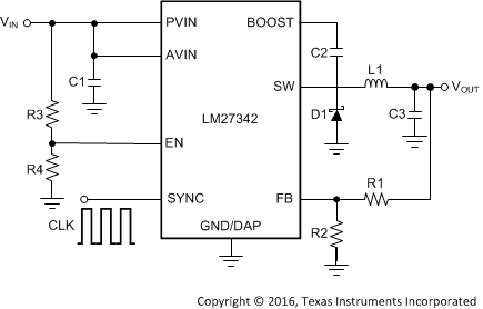 Figure 30. Resistor Divider on EN

7.4.2 Soft-Start Mode
The LM2734x and LM2734x-Q1 have a fixed internal soft-start of 1 ms (typical). During soft start, the error amplifier’s reference voltage ramps from 0 V to its nominal value of 1 V in approximately 1 ms. This forces the regulator output to ramp in a controlled fashion, which helps reduce inrush current. Upon soft start, the part is initially in frequency foldback and the frequency rises as FB rises. The regulator rises gradually to 2 MHz. The LM2734x and LM2734x-Q1 allows synchronization to an external clock at FB > 0.53 V.