SNVS316H September 2004 – December 2014 LM2736
PRODUCTION DATA.
- 1 Features
- 2 Applications
- 3 Description
- 4 Revision History
- 5 Pin Configuration and Functions
- 6 Specifications
- 7 Detailed Description
-
8 Application and Implementation
- 8.1 Application Information
- 8.2
Typical Applications
- 8.2.1 LM2736X (1.6 MHz) VBOOST Derived from VIN 5 V to 1.5 V / 750 mA
- 8.2.2 LM2736X (1.6 MHz) VBOOST Derived from VOUT 12 V to 3.3 V / 750 mA
- 8.2.3 LM2736X (1.6 MHz) VBOOST Derived from VSHUNT 18 V to 1.5 V / 750 mA
- 8.2.4 LM2736X (1.6 MHz) VBOOST Derived from Series Zener Diode (VIN) 15 V to 1.5 V / 750 mA
- 8.2.5 LM2736X (1.6 MHz) VBOOST Derived from Series Zener Diode (VOUT) 15 V to 9 V / 750 mA
- 8.2.6 LM2736Y (550 kHz) VBOOST Derived from VIN 5 V to 1.5 V / 750 mA
- 8.2.7 LM2736Y (550 kHz) VBOOST Derived from VOUT 12 V to 3.3 V / 750 mA
- 8.2.8 LM2736Y (550 kHz) VBOOST Derived from VSHUNT 18 V to 1.5 V / 750 mA
- 8.2.9 LM2736Y (550 kHz) VBOOST Derived from Series Zener Diode (VIN) 15 V to 1.5 V / 750 mA
- 8.2.10 LM2736Y (550 kHz) VBOOST Derived from Series Zener Diode (VOUT) 15 V to 9 V / 750 mA
- 9 Power Supply Recommendations
- 10Layout
- 11Device and Documentation Support
- 12Mechanical, Packaging, and Orderable Information
Package Options
Mechanical Data (Package|Pins)
- DDC|6
Thermal pad, mechanical data (Package|Pins)
Orderable Information
5 Pin Configuration and Functions
Package DDC (R-PDSO-G6)
6-Lead SOT
Top View
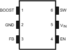
Pin Functions
| PIN | I/O | DESCRIPTION | |
|---|---|---|---|
| NAME | NO. | ||
| BOOST | 1 | I | Boost voltage that drives the internal NMOS control switch. A bootstrap capacitor is connected between the BOOST and SW pins. |
| GND | 2 | GND | Signal and Power ground pin. Place the bottom resistor of the feedback network as close as possible to this pin for accurate regulation. |
| FB | 3 | I | Feedback pin. Connect FB to the external resistor divider to set output voltage. |
| EN | 4 | I | Enable control input. Logic high enables operation. Do not allow this pin to float or be greater than VIN + 0.3 V. |
| VIN | 5 | I | Input supply voltage. Connect a bypass capacitor to this pin. |
| SW | 6 | O | Output switch. Connects to the inductor, catch diode, and bootstrap capacitor. |