SNVS896B August 2013 – November 2014 LM27403
PRODUCTION DATA.
- 1 Features
- 2 Applications
- 3 Description
- 4 Revision History
- 5 Description (Continued)
- 6 Pin Configuration and Functions
- 7 Specifications
-
8 Detailed Description
- 8.1 Overview
- 8.2 Functional Block Diagram
- 8.3
Feature Description
- 8.3.1 Input Range: VIN
- 8.3.2 Output Voltage: FB Voltage and Accuracy
- 8.3.3 Input and Bias Rail Voltages: VIN and VDD
- 8.3.4 Precision Enable: UVLO/EN
- 8.3.5 Switching Frequency
- 8.3.6 Temperature Sensing: D+ and D-
- 8.3.7 Thermal Shutdown: OTP
- 8.3.8 Inductor-DCR-Based Overcurrent Protection
- 8.3.9 Current Sensing: CS+ and CS-
- 8.3.10 Current Limit Handling
- 8.3.11 Soft-Start: SS/TRACK
- 8.3.12 Monotonic Startup
- 8.3.13 Prebias Startup
- 8.3.14 Voltage-Mode Control
- 8.3.15 Output Voltage Remote Sense: RS
- 8.3.16 Power Good: PGOOD
- 8.3.17 Gate Drivers: LG and HG
- 8.3.18 Sink and Source Capability
- 8.4 Device Functional Modes
-
9 Application and Implementation
- 9.1 Application Information
- 9.2
Typical Applications
- 9.2.1 Design 1 - High-Efficiency Synchronous Buck Regulator for Telecom Power
- 9.2.2 Design 2 - Powering FPGAs Using Flexible 30A Regulator With Small Footprint
- 9.2.3 Design 3 - Powering Multicore DSPs
- 9.2.4 Design 4 - Regulated 12-V Rail with LDO Low-Noise Auxiliary Output for RF Power
- 9.2.5 Design 5 - High Power Density Implementation From 3.3-V or 5-V Supply Rail
- 10Power Supply Recommendations
- 11Layout
- 12Device and Documentation Support
- 13Mechanical, Packaging, and Orderable Information
Package Options
Mechanical Data (Package|Pins)
- RTW|24
Thermal pad, mechanical data (Package|Pins)
- RTW|24
Orderable Information
9 Application and Implementation
NOTE
Information in the following applications sections is not part of the TI component specification, and TI does not warrant its accuracy or completeness. TI’s customers are responsible for determining suitability of components for their purposes. Customers should validate and test their design implementation to confirm system functionality.
9.1 Application Information
9.1.1 Design and Implementation
To expedite the process of designing of a LM27403-based regulator for a given application, please use the LM27403 Quick-start Design Tool available as a free download. As well as numerous LM27403 reference designs populated in TI Designs™ reference design library, five designs are provided in the Typical Applications section of this datasheet. The LM27403 is also WEBENCH® Designer enabled.
9.1.2 Power Train Components
Comprehensive knowledge and understanding of the power train components are key to successfully completing a buck regulator design. The LM27403 Design Tool and WEBENCH are available to assist the designer with selection of these components for a given application.
9.1.2.1 Filter Inductor
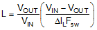
For most applications, choose an inductance such that the inductor ripple current, ΔIL, is between 20% and 40% of the maximum dc output current. Choose the inductance using Equation 10:
Check the inductor datasheet to ensure that the inductor's saturation current is well above the peak inductor current of a particular design. Ferrite designs have very low core loss and are preferred at high switching frequencies, so design goals can then concentrate on copper loss and preventing saturation. Low inductor core loss is evidenced by reduced no-load input current and higher light-load efficiency. However, ferrite core materials exhibit a hard saturation characteristic – the inductance collapses abruptly when the saturation current is exceeded. This results in an abrupt increase in inductor ripple current, higher output voltage ripple, not to mention reduced efficiency and compromised reliability. Note that an inductor's saturation current generally deceases as its core temperature increases. Of course, accurate overcurrent protection is key to avoiding inductor saturation.
9.1.2.2 Output Capacitors
Ordinarily, the regulator’s output capacitor energy store combined with the control loop response are prescribed to maintain the integrity of the output voltage within both the static and dynamic (transient) tolerance specifications. The usual boundaries restricting the output capacitor in power management applications are driven by finite available PCB area, component footprint and profile, and cost. The capacitor parasitics – equivalent series resistance (ESR) and equivalent series inductance (ESL) – take increasing precedence in shaping the regulator’s load transient response as the output current ramp amplitude and slew rate increase.
So, the output capacitor, COUT, exists to filter the inductor ripple current and provide a reservoir of charge for step load transient events. Typically, ceramic capacitors provide extremely low ESR to reduce the output voltage ripple and noise spikes, while tantalum and electrolytic capacitors provide a large bulk capacitance in a relatively compact footprint for transient loading events.
Based on the static specification of peak-to-peak output voltage ripple denoted by ΔVO, choose an output capacitance that is larger than
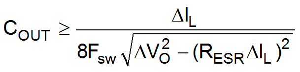
Figure 38 conceptually illustrates the relevant current waveforms during both load step-up and step-down transitions. As shown, the large-signal slew rate of the inductor current is limited as the inductor current ramps to match the new load-current level following a load transient. This slew-rate limiting exacerbates the deficit of charge in the output capacitor, which must be replenished as rapidly as possible during and after the load-on transient. Similarly, during and after a load-off transient, the slew rate limiting of the inductor current adds to the surplus of charge in the output capacitor that needs to be depleted as quickly as possible.
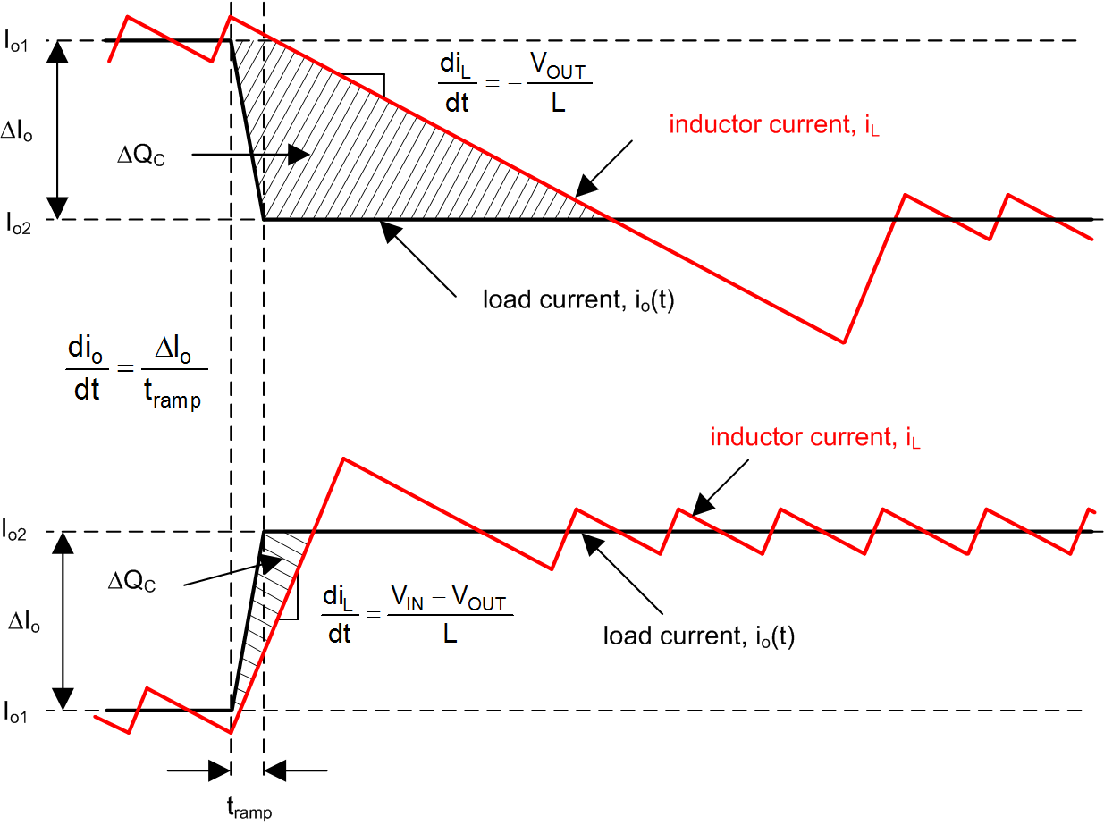 Figure 38. Load Transient Response Representation Showing COUT Charge Surplus Or Deficit.
In a typical regulator application of 12-V input to low output voltage (say 1.2 V), it should be recognized that the load-off transient represents worst-case. In that case, the steady-state duty cycle is approximately 10% and the large-signal inductor current slew rate when the duty cycle collapses to zero is approximately –VOUT/L. Compared to a load-on transient, the inductor current takes much longer to transition to the required level. The surplus of charge in the output capacitor causes the output voltage to significantly overshoot. In fact, to deplete this excess charge from the output capacitor as quickly as possible, the inductor current must ramp below its nominal level following the load step. In this scenario, a large output capacitance can be advantageously employed to absorb the excess charge and rein in the voltage overshoot.
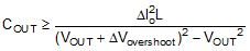
To meet the dynamic specification of output voltage overshoot during such a load-off transient (denoted as ΔVovershoot with step reduction in output current given by ΔIo), the output capacitance should be larger than
The ESR of a capacitor is provided in the manufacturer’s datasheet either explicitly as a specification or implicitly in the impedance vs. frequency curve. Depending on type, size and construction, electrolytic capacitors have significant ESR, 5 mΩ and above, and relatively large ESL, 5 nH to 20 nH. PCB traces contribute some ESR and ESL as well. Ceramic output capacitors, on the other hand, are such that the impedances related to the ESR and ESL are small at the switching frequency, and the capacitive impedance dominates. However, depending on package and voltage rating of the ceramic capacitor, the effective capacitance can drop quite significantly with applied voltage and operating temperature.
Ignoring the ESR term in Equation 11 gives a quick estimation of the minimum ceramic capacitance necessary to meet the output ripple specification. One to four 100-µF, 6.3-V, X5R capacitors in 1206 or 1210 footprint is a common choice. Use Equation 12 to quantify if additional capacitance is necessary to meet the load-off transient overshoot specification.
A composite implementation of ceramic and electrolytic capacitors highlights the rationale of paralleling capacitors of dissimilar chemistries yet complementary performance. The frequency response of each capacitor is accretive in that each capacitor provides desirable performance over a certain portion of the frequency range of interest. While the ceramic provides excellent mid- and high-frequency decoupling characteristics with its low ESR and ESL to minimize the switching frequency output ripple, the electrolytic device with its large bulk capacitance provides low-frequency energy storage to cope with load-transient demands.
9.1.2.3 Input Capacitors
Input capacitors are necessary to limit the input ripple voltage while switching-frequency ac current to the buck power stage. It is generally recommended to use X5R or X7R dielectric ceramic capacitors, thus providing low impedance and high RMS current rating over a wide temperature range. To minimize the parasitic inductance in the switching loop, position the input capacitors as close as possible to the drain of the high-side MOSFET and the source of the low-side MOSFET.
The input capacitors' RMS current is given by Equation 13.
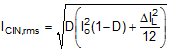
The highest requirement for input capacitor RMS current rating occurs at D = 0.5, at which point the RMS current rating should be greater than half the output current.
Ideally, the dc component of input current is provided by the input voltage source and the ac component by the input filter capacitors. Neglecting inductor ripple current, the input capacitors source current of amplitude Io−IIN during the D interval and sinks IIN during the 1−D interval. Thus, the input capacitors conduct a square-wave current of peak-to-peak amplitude equal to the output current. It follows that the resultant capacitive component of ac ripple voltage is a triangular waveform. Together with the ESR-related ripple component, the peak-to-peak ripple voltage amplitude is given by Equation 14.
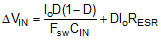
The input capacitance required for a particular load current, based on an input voltage ripple specification of ΔVIN, is given by Equation 15.
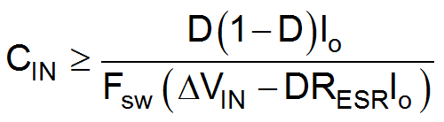
Low ESR ceramic capacitors can be placed in parallel with higher valued bulk capacitance to provide optimized input filtering for the regulator and damping to mitigate the effects of input parasitic inductance resonating with high-Q ceramics. One bulk capacitor of sufficiently high current rating and one or two 10-μF 25-V X7R ceramic decoupling capacitors are usually sufficient. Select the input bulk capacitor based on its ripple current rating and operating temperature.
9.1.2.4 Power MOSFETs
The choice of MOSFET has significant impact on DC-DC regulator performance. A MOSFET with low on-state resistance, RDS(on), reduces conduction loss, whereas low parasitic capacitances enable faster transition times and reduced switching loss. Normally, the lower the RDS(on) of a MOSFET, the higher the gate charge, QG, and vice versa. As a result, the product RDS(on)*QG is commonly specified as a MOSFET figure-of-merit. Low thermal resistance ensures that the MOSFET power dissipation does not result in excessive MOSFET die temperature.
The main parameters affecting MOSFET selection in an LM27403 application are as follows:
- RDS(on) at VGS = 4.5 V;
- Drain-source voltage rating, BVDSS, typically 25 V or 30 V;
- Gate charge parameters at VGS = 4.5 V;
- Body diode reverse recovery charge, QRR;
- Gate threshold voltage, VGS(th), derived from the plateau in the QG vs. VGS curve in the MOSFET's datasheet. VGS(th) should be in the range 2 V to 3 V such that the MOSFET is adequately enhanced when on and margin against Cdv/dt shoot-through exists when off.
The MOSFET-related power losses are summarized by the equations presented in Table 2. While the influence of inductor ripple current is considered, second-order loss modes, such as those related to parasitic inductances, are not discussed. Consult the LM27403 Quick-start Design Tool to assist with power loss calculations.
Table 2. Buck Regulator MOSFET Power Losses
| Power Loss Mode | High-Side MOSFET | Low-Side MOSFET |
|---|---|---|
| Conduction (2) | 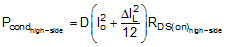 |
 (3) (3) |
| Switching | 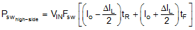 |
Negligible |
| Gate Drive(1) | 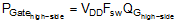 |
 |
| Body Diode Conduction | N/A | 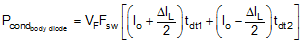 |
| Body Diode Reverse Recovery |  |
|
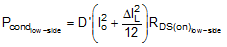
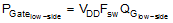
The high-side (control) MOSFET carries the inductor current during the PWM on time (or D interval) and typically incurs most of the switching losses. It is therefore imperative to choose a high-side MOSFET that balances conduction and switching loss contributions. The total power dissipation in the high-side MOSFET is the sum of the losses due to conduction, switching and typically two-thirds of the net loss attributed to body diode reverse recovery.
The low-side (synchronous) MOSFET carries the inductor current when the high-side MOSFET is off (or 1–D interval). The low-side MOSFET switching loss is negligible as it is switched at zero voltage – current just commutates from the channel to the body diode or vice versa during the deadtime. The LM27403, with its adaptive gate drive timing, minimizes body diode conduction losses when both MOSFETs are off. Such losses scale directly with switching frequency.
In high input voltage and low output voltage applications, the low-side MOSFET carries the current for a large portion of the switching period. Therefore, to attain high efficiency, it is critical to optimize the low-side MOSFET for low RDS(on). In cases where the conduction loss is too high or the target RDS(on) is lower than available in a single MOSFET, connect two low-side MOSFETs in parallel. The total power dissipation of the low-side MOSFET is the sum of the losses due to channel conduction, body diode conduction, and typically one-third of the net loss attributed to body diode reverse recovery.
The LM27403 is well matched to TI's comprehensive portfolio of 25-V and 30-V NexFET™ family of power MOSFETs. In fact, the LM27403 is ideally suited to driving the Power Block NexFET™ modules with integrated high-side and low-side MOSFETs. Excellent efficiency is obtained by virtue of reduced parasitics and exemplary thermal performance of the Power Block MOSFET implementation. See the Typical Applications section for more details.
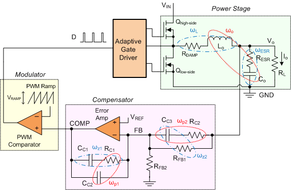
9.1.3 Control Loop Compensation
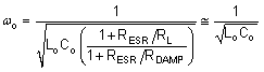
The poles and zeros inherent to the power stage and compensator are respectively illustrated by red and blue dashed rings in the schematic embedded in Table 3.
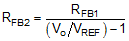
The compensation network typically employed with voltage-mode control is a type-III circuit with three poles and two zeros. One compensator pole is located at the origin to realize high DC gain. The normal compensation strategy then is to use two compensator zeros to counteract the LC double pole, one compensator pole located to nullify the output capacitor ESR zero, with the remaining compensator pole located at one-half switching frequency to attenuate high frequency noise. Finally, a resistor divider network to FB determines the desired output voltage. Note that the lower feedback resistor, RFB2, has no impact on the control loop from an ac standpoint since the FB node is the input to an error amplifier and is effectively at ac ground. Hence, the control loop is designed irrespective of output voltage level. The proviso here is the necessary output capacitance derating with bias voltage and temperature.
Table 3. Regulator Poles and Zeros
|
|||
|---|---|---|---|
| Power Stage Poles | Power Stage Zeros | Compensator Poles | Compensator Zeros |
 |
 (1) (1) |
 |
 |
 (2) (2) |
 |
 |
|
The small-signal open-loop response of a buck regulator is the product of modulator, power train and compensator transfer functions. The power stage transfer function can be represented as a complex pole pair associated with the output LC filter and a zero related to the output capacitor's ESR. The dc (and low frequency) gain of the modulator and power stage is VIN/VRAMP. Representing the gain from COMP to the average voltage at the input of the LC filter, this is held essentially constant by the LM27403's PWM line feedforward feature at 9 V/V or 19 dB.
Complete expressions for small-signal frequency analysis are presented in Table 4. The transfer functions are denoted in normalized form. While the loop gain is of primary importance, a regulator is not specified directly by its loop gain but by its performance related characteristics, namely closed-loop output impedance and audio susceptibility.
Table 4. Buck Regulator Small-Signal Analysis
| PARAMETER | EXPRESSION |
|---|---|
| Open-loop transfer function |  |
| Duty-cycle-to-output transfer function |  |
| Compensator transfer function(1) | 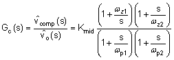 |
| Modulator transfer function | 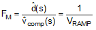 |
An illustration of the open-loop response gain and phase is given in Figure 39. The poles and zeros of the system are marked with x and o symbols, respectively, and a + symbol indicates the crossover frequency. When plotted on a log (dB) scale, the open-loop gain is effectively the sum of the individual gain components from the modulator, power stage and compensator – this is clear from Figure 40. The open-loop response of the system is measured experimentally by breaking the loop, injecting a variable-frequency oscillator signal and recording the ensuing frequency response using a network analyzer setup.
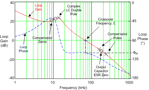 Figure 39. Typical Buck Regulator Loop Gain and Phase With Voltage-Mode Control
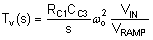
If the pole located at ωp1 cancels the zero located at ωESR and the pole at ωp2 is located well above crossover, the expression for the loop gain, Tv(s) in Table 4, can be manipulated to yield the simplified expression given in Equation 16.
Essentially, a multi-order system is reduced to a single order approximation by judicious choice of compensator components. A simple solution for the crossover frequency, denoted as fc in Figure 39, with type-III voltage-mode control is derived as in Equation 17.
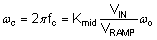
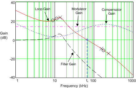 Figure 40. Buck Regulator Constituent Gain Components
The loop crossover frequency is usually selected between one-tenth to one-fifth of switching frequency. Inserting an appropriate crossover frequency into Equation 17 gives a target for the compensator's mid-band gain, Kmid. Given an initial value for RFB1, RFB2 is then selected based on the desired output voltage. Values for RC1, RC2, CC1, CC2 and CC3 are calculated from the design-oriented expressions listed in Table 5, with the premise that the compensator poles and zeros are set as follows: ωz1 = 0.5ωo, ωz2 = ωo, ωp1 = ωESR, ωp2 = ωsw/2.
Table 5. Compensation Component Selection
| RESISTORS | CAPACITORS |
|---|---|
 |
 |
 |
 |
 |
 |
Referring to the bode plot in Figure 39, the phase margin, indicated as φM, is the difference between the loop phase and –180° at crossover. A target of 50° to 70° for this parameter is considered ideal. Additional phase boost is dialed in by locating the compensator zeros at a frequency lower than the LC double pole (hence why CC1 is scaled by a factor of 2 above). This helps to mitigate the phase dip associated with the LC filter, particularly at light loads when the Q-factor is higher and the phase dip becomes especially prominent. The ramification of low phase in the frequency domain is an under-damped transient response in the time domain.
The power supply designer now has all the tools at his/her disposal to optimally position the loop crossover frequency while maintaining adequate phase margin over the power supply's required line, load and temperature operating ranges.
9.2 Typical Applications
9.2.1 Design 1 - High-Efficiency Synchronous Buck Regulator for Telecom Power
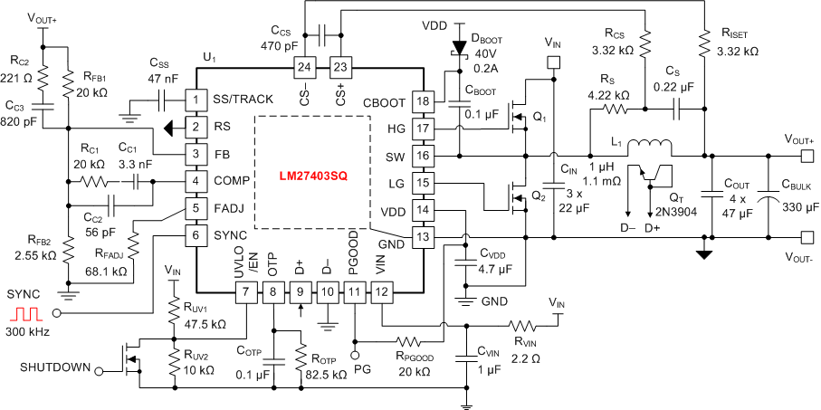 Figure 41. Application Circuit 1 with VIN = 6.5 V to 20 V (VIN(nom) = 12 V), VOUT = 0.6 V to 5.3 V, IOUT(max) = 25 A, FSW = 300 kHz (Using External Synchronization Signal)
9.2.1.1 Design Requirements
The schematic diagram of a 25-A regulator is given in Figure 41. In this example, the target full-load efficiencies are 91% and 97% at 1.2-V and 5.3-V output voltages, respectively, based on a nominal input voltage of 12 V that ranges from 6.5 V to 20 V. Output voltage is adjusted simply by changing RFB2. The switching frequency is set by means of a synchronization signal at 300 kHz, and free-running switching frequency (in the event that the synchronization signal is removed) is set to 250 kHz by resistor RFADJ. In terms of control loop performance, the target loop crossover frequency is 45 kHz with a phase margin in excess of 50°. The output voltage soft-start time is 8 ms.
9.2.1.2 Detailed Design Procedure
The design procedure for an LM27403-based converter for a given application is streamlined by using the LM27403 Quick-Start Design Tool available as a free download, or by availing of TI's WEBENCH® Designer online software. Such tools are complemented by the availability of two LM27403 evaluation module (EVM) designs as well as numerous LM27403 reference designs populated in TI Designs™ reference design library.
The current limit setpoint in this design is set at 28.5 A, based on resistor RISET and the inductor DCR (1.1 mΩ typ at 25°C). Of course, the current limit setpoint should always be selected such that the operating current level does not exceed the saturation current specification of the chosen inductor. The component values for the DCR sense network (RS and CS in Figure 41) are chosen based on making the RSCS product approximately equal to L/Rdcr, as recommended in the Current Sensing: CS+ and CS– section.
The selected buck converter powertrain components are cited in Table 6, and many of the components are available from multiple vendors. The MOSFETs in particular are chosen for both lowest conduction and switching power loss, as discussed in detail in the Power MOSFETs section.
Table 6. List of Materials for Design 1
| REFERENCE DESIGNATOR | QTY | SPECIFICATION | MANUFACTURER | PART NUMBER |
|---|---|---|---|---|
| CIN | 3 | 22 µF, 25 V, X7R, 1210 ceramic | Kemet | C1210C226M3RACTU |
| Taiyo Yuden | TMK325B7226MM-TR | |||
| Murata | GRM32ER71E226KE15L | |||
| COUT | 4 | 47 µF, 10 V, X7R, 1210 ceramic | Taiyo Yuden | LMK325B7476MM-TR |
| Murata | GRM32ER71A476KE15L | |||
| CBULK | 1 | 330 µF, 6.3 V, 9 mΩ, D3L POSCAP | Sanyo | 6TPF330M9L |
| L1 | 1 | 1.0 µH, 30 A, 1.1 mΩ ±10%, ferrite | Delta | HMP1360-1R0-63 |
| Q1 | 1 | 25 V, high-side MOSFET | Infineon | BSC032NE2LS |
| Texas Instruments | CSD16322Q5 | |||
| Q2 | 1 | 25 V, low-side MOSFET | Infineon | BSC010NE2LS |
| Texas Instruments | CSD16415Q5 |
9.2.1.3 Application Curves
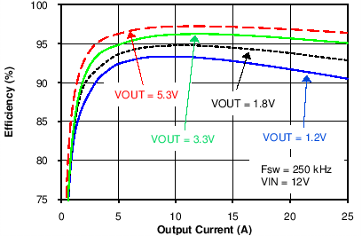 Figure 42. Efficiency vs. Output Current at VIN = 12 V
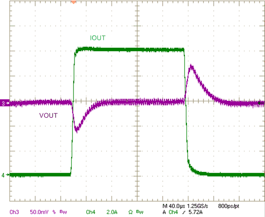 Figure 44. Load Transient Response at VOUT = 1.2 V, IOUT 0A to 10A at 2A/µs
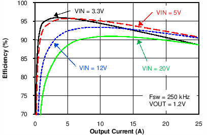 Figure 43. Efficiency vs. Output Current at VOUT = 1.2 V
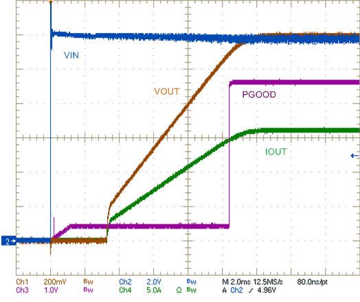 Figure 45. Startup Characteristic with VIN stepped from 0 V to 12 V, VOUT = 1.2 V, 70-mΩ Load
9.2.2 Design 2 - Powering FPGAs Using Flexible 30A Regulator With Small Footprint
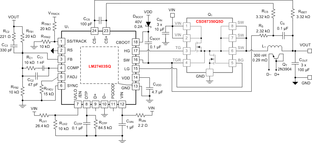 Figure 46. Application Circuit 2 With VIN = 4.5 V to 15 V (VIN(nom) = 12 V), VOUT = 1.8 V, IOUT(max) = 30 A, FSW = 600 kHz
9.2.2.1 Design Requirements
The schematic diagram of a 600-kHz, 30-A regulator is given in Figure 46. The powertrain components are listed in Table 7.
Table 7. List of Materials for Design 2
| REFERENCE DESIGNATOR | QTY | SPECIFICATION | MANUFACTURER | PART NUMBER | |
|---|---|---|---|---|---|
| CIN | 3 | 10 µF, 25 V, X5R, 0805 ceramic | Taiyo Yuden | TMK212BBJ106KG-T | |
| Murata | GRM21BR61E106KA73L | ||||
| TDK | C2012X5R1E106M | ||||
| COUT | 1 | 100 µF, 6.3 V, X5R, 1206 ceramic | Taiyo Yuden | JMK316BJ107ML-T | |
| Murarta | GRM31CR60J107ME39L | ||||
| TDK | C3216X5R0J107M | ||||
| Kemet | C1206C107M9PACTU | ||||
| L1 | 1 | 300 nH, ferrite | 35 A, 0.29 mΩ ±8% | Coiltronics | FP1107R1-R30-R |
| 34 A, 0.29 mΩ ±7% | Cyntec | PCDC1107-R30EMO | |||
| 270 nH, ferrite | 37 A, 0.24 mΩ ±5% | Coilcraft | SLC1175-271MEC | ||
| 250 nH, ferrite | 44 A, 0.37 mΩ ±7% | Wurth | 744308025 | ||
| Q1 | 1 | 30 V Power Block Q5D MOSFET Module, 5 mm x 6 mm | Texas Instruments | CSD87350Q5D | |
9.2.2.2 Detailed Design Procedure
A high power density, high efficiency solution is feasible by using TI NexFET™ Power Block module CSD87350Q5D (dual asymmetric MOSFETs in a SON 5-mm x 6-mm package) together with and low-DCR ferrite inductor and all-ceramic capacitor design. The design occupies 20 mm x 15 mm on a single-sided PCB. Knowing the cumulative resistance of the inductor DCR and Power Block MOSFET SW clip (approximately 1 mΩ at 25°C), resistor RISET positions the current limit setpoint at 28A. The output voltage is adjusted by choosing the resistance of RFB2 appropriately. Resistors RTRK1 and RTRK2 connected to the SS/TRACK pin define a coincidental tracking startup sequence from a master power supply, VTRACK.
Additional input and/or output capacitance can be added if needed, but adjust the compensation if COUT changes. The TGR pin of the Power Block MOSFET serves as a kelvin connection to the source of the high-side MOSFET and represents the return path for the high-side gate drive. Along with bootstrap capacitor, CBOOT, TGR is connected to the LM27403's SW pin.
9.2.2.3 Application Curves
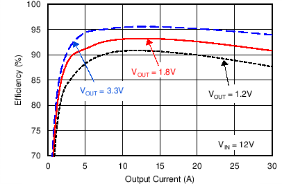 Figure 47. Efficiency vs. Output Current at VIN = 12 V
9.2.3 Design 3 - Powering Multicore DSPs
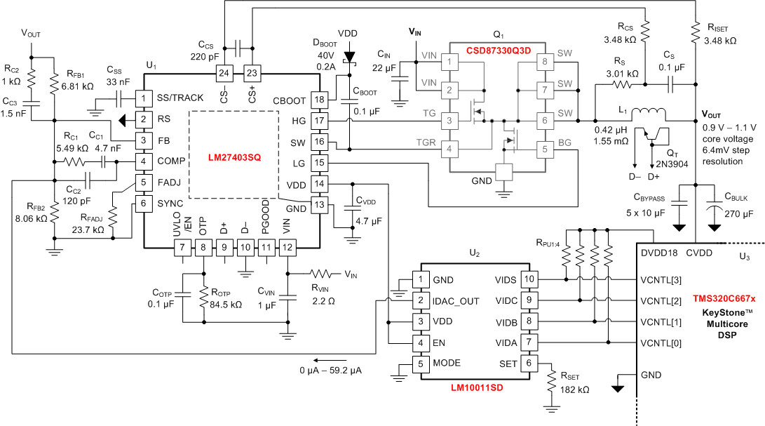 Figure 48. Application Circuit 3 with VIN = 3 V to 20 V, VOUT = 0.9 V to 1.1 V, IOUT(max) = 15 A, FSW = 450 kHz
The schematic diagram of a 450-kHz, 12-V nominal input, 15-A regulator powering a KeyStone™ DSP is given in Figure 48. The important components are listed in Table 8. The regulator output current requirements are dependent upon the baseline and activity power consumptions of the DSP in a real-use case. While baseline power is highly dependent on voltage, temperature and DSP frequency, activity power relates to dynamic core utilization, DDR3 memory access, peripherals, and so on. To this end, the IDAC_OUT pin of the LM10011 connects to the LM27403 FB pin to allow continuous optimization of the core voltage. The SmartReflex-enabled DSP provides 6-bit information using the VCNTL open-drain IOs(1) to command the output voltage setpoint with 6.4-mV step resolution. This design uses a TI NexFET™ Power Block module CSD87330Q3D (dual asymmetric MOSFETs in SON 3.3-mm x 3.3-mm package) together with low-DCR, metal-powder inductor and composite ceramic–polymer electrolytic output capacitor implementation.
Table 8. List of Materials for Design 3
| REFERENCE DESIGNATOR | QTY | SPECIFICATION | MANUFACTURER | PART NUMBER |
|---|---|---|---|---|
| CIN | 1 | 22 µF, 25 V, X5R, 1210 ceramic | Taiyo Yuden | TMK325BJ226MM-T |
| CBYPASS | 5 | 10 µF, 4 V, X5R, 0402 ceramic | Taiyo Yuden | AMK105BJ106MV-F |
| CBULK | 1 | 270 µF, 2 V, 6 mΩ, 3.2 Arms, 3.5 mm x 2.8 mm, POSCAP | Panasonic | 2TPSF270M6E |
| L1 | 1 | 0.42 µH, 22 A, 1.55 mΩ ±7%, molded, 6.9 mm x 6.6 mm | Cyntec | PIME064T-R42MS1R557 |
| Q1 | 1 | 30 V Power Block Q3D MOSFET Module, 3.3 mm x 3.3 mm | Texas Instruments | CSD87330Q3D |
| QT | 1 | 2N3904 type NPN transistor, 40 V, 0.2 A, SOT-523 | Diodes, Inc. | MMBT3904T |
| U2 | 1 | 6- or 4-bit VID Programmable Current DAC, WSON-10 | Texas Instruments | LM10011SD |
| U3 | 1 | KeyStone™ DSP | Texas Instruments | TMS320C667x |
9.2.4 Design 4 - Regulated 12-V Rail with LDO Low-Noise Auxiliary Output for RF Power
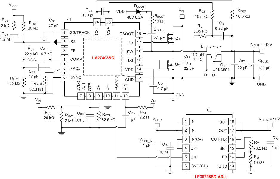 Figure 49. Application Circuit 4 with VIN = 13 V to 20 V (VIN(nom) = 18 V), VOUT1 = 12 V, IOUT1(max) = 10 A, FSW = 280 kHz, VOUT2 = 10 V, IOUT2(max) = 0.8 A
The schematic diagram of a 280-kHz, 12-V output, 10-A buck regulator for RF power applications is given in Figure 49(1). A 10-Ω resistor in series with CBOOT is used to slow the turn-on transition of the high-side MOSFET, reducing the spike amplitude and ringing of the SW node waveform and minimizing the possibility of Cdv/dt-induced shoot-through of the low-side MOSFET. If needed, place an RC snubber (for example, 2.2 Ω and 1 nF) close to the SW node and GND(2). An auxiliary 10-V, 800-mA rail to power noise-sensitive circuits is available using the LP38798 ultra-low noise LDO as a post-regulator. The internal pullup of the LP38798's EN pin facilitates direct connection to the LM27403's PGOOD for sequential startup control.
Table 9. List of Materials for Design 4
| REFERENCE DESIGNATOR | QTY | SPECIFICATION | MANUFACTURER | PART NUMBER |
|---|---|---|---|---|
| CIN | 3 | 22 µF, 25 V, X5R, 1210 ceramic | Taiyo Yuden | TMK325BJ226MM-T |
| CBYP | 1 | 22 µF, 16 V, X7R, 1210 ceramic | Taiyo Yuden | EMK325B7226MM-T |
| CBULK | 1 | 180 µF, 16 V, 22 mΩ, 3.3 Arms, C6, OSCON | Panasonic | 16SVPF180M |
| L1 | 1 | 4.7 µH, 15 A, 7 mΩ, flat wire high current | Wurth | 7443551470 |
| Q1 | 1 | 30 V, high-side MOSFET | Texas Instruments | CSD17309Q3 |
| Q2 | 1 | 30 V, low-side MOSFET | Infineon | BSC011NE3LS |
| U2 | 1 | Ultra-Low Noise, High PSRR LDO for RF/Analog Circuits, 4-mm x 4-mm WSON-12 | Texas Instruments | LP38798SD-ADJ |
9.2.5 Design 5 - High Power Density Implementation From 3.3-V or 5-V Supply Rail
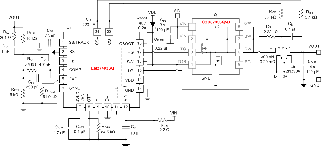 Figure 50. Application Circuit 5 With VIN = 3.3 V to 5.5 V, VOUT = 1 V, IOUT(max) = 25 A, FSW = 250 kHz
The schematic diagram of a 250-kHz, 25-A regulator is given in Figure 50. A high power density, ultra-high efficiency solution is possible using two paralleled TI CSD87353Q5D NexFET™ Power Block modules (dual MOSFETs in a SON 5-mm x 6-mm package) and low-DCR ferrite inductor. The design occupies 25 mm x 15 mm on a two-sided PCB. Knowing the cumulative resistance of the inductor DCR and Power Block MOSFET SW clip (approximately 0.8 mΩ at 25°C), resistor RISET positions the current limit setpoint at 30A. VDD is tied to VIN to maximize the gate drive voltage for the MOSFETs. Capacitor CDLY defines a 3-ms startup delay based on the current sourced from the UVLO/EN pin.
The powertrain components are listed in Table 10, and the filter components are available from multiple vendors. The TGR pin of the Power Block MOSFET serves as a kelvin connection to the source of the high-side MOSFET and represents the return path for the high-side gate drive. Along with bootstrap capacitor, CBOOT, TGR is connected to the LM27403's SW pin.
Table 10. List of Materials for Design 5
| REFERENCE DESIGNATOR | QTY | SPECIFICATION | MANUFACTURER | PART NUMBER | |
|---|---|---|---|---|---|
| CIN | 3 | 100 µF, 6.3 V, X5R, 1210 ceramic | Kemet | C1210C107M9PACTU | |
| TDK | C3225X5R0J107M | ||||
| Murata | GRM32ER60J107ME20K | ||||
| COUT | 4 | 100 µF, 6.3 V, X5R, 1206 ceramic | Taiyo Yuden | JMK316BJ107ML-T | |
| Murarta | GRM31CR60J107ME39L | ||||
| TDK | C3216X5R0J107M | ||||
| Kemet | C1206C107M9PACTU | ||||
| L1 | 1 | 300 nH, ferrite | 35 A, 0.29 mΩ ±8% | Coiltronics | FP1107R1-R30-R |
| 330 nH, ferrite | 46 A, 0.32 mΩ ±7% | Wurth Electronik | 744301033 | ||
| Q1 | 2 | 30 V Power Block Q5D MOSFET Module, 5 mm x 6 mm | Texas Instruments | CSD87353Q5D | |