SNVS896B August 2013 – November 2014 LM27403
PRODUCTION DATA.
- 1 Features
- 2 Applications
- 3 Description
- 4 Revision History
- 5 Description (Continued)
- 6 Pin Configuration and Functions
- 7 Specifications
-
8 Detailed Description
- 8.1 Overview
- 8.2 Functional Block Diagram
- 8.3
Feature Description
- 8.3.1 Input Range: VIN
- 8.3.2 Output Voltage: FB Voltage and Accuracy
- 8.3.3 Input and Bias Rail Voltages: VIN and VDD
- 8.3.4 Precision Enable: UVLO/EN
- 8.3.5 Switching Frequency
- 8.3.6 Temperature Sensing: D+ and D-
- 8.3.7 Thermal Shutdown: OTP
- 8.3.8 Inductor-DCR-Based Overcurrent Protection
- 8.3.9 Current Sensing: CS+ and CS-
- 8.3.10 Current Limit Handling
- 8.3.11 Soft-Start: SS/TRACK
- 8.3.12 Monotonic Startup
- 8.3.13 Prebias Startup
- 8.3.14 Voltage-Mode Control
- 8.3.15 Output Voltage Remote Sense: RS
- 8.3.16 Power Good: PGOOD
- 8.3.17 Gate Drivers: LG and HG
- 8.3.18 Sink and Source Capability
- 8.4 Device Functional Modes
-
9 Application and Implementation
- 9.1 Application Information
- 9.2
Typical Applications
- 9.2.1 Design 1 - High-Efficiency Synchronous Buck Regulator for Telecom Power
- 9.2.2 Design 2 - Powering FPGAs Using Flexible 30A Regulator With Small Footprint
- 9.2.3 Design 3 - Powering Multicore DSPs
- 9.2.4 Design 4 - Regulated 12-V Rail with LDO Low-Noise Auxiliary Output for RF Power
- 9.2.5 Design 5 - High Power Density Implementation From 3.3-V or 5-V Supply Rail
- 10Power Supply Recommendations
- 11Layout
- 12Device and Documentation Support
- 13Mechanical, Packaging, and Orderable Information
Package Options
Mechanical Data (Package|Pins)
- RTW|24
Thermal pad, mechanical data (Package|Pins)
- RTW|24
Orderable Information
6 Pin Configuration and Functions
24-Pins
WQFN Package
(Top View)
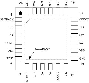
Pin Functions
| PIN | I/O/P(1) | DESCRIPTION | |
|---|---|---|---|
| NAME | NO. | ||
| CBOOT | 18 | P | High-side bootstrap connection. This pin is the high-side N-FET gate driver power supply. Connect a 100-nF ceramic capacitor between CBOOT and SW. |
| COMP | 4 | O | Compensation node output. This pin is an output voltage control-loop error amplifier output. COMP is connected to the FB pin through a compensation network to ensure stability. |
| CS– | 24 | I | Current-sense negative input. This pin is the inverting input to the current-sense comparator. 9.9 µA of nominal offset current at room temperature is provided to adjust the current limit setpoint. |
| CS+ | 23 | I | Current-sense positive input. This pin is the noninverting input to the current-sense comparator. |
| D– | 10 | I | External temperature sense return. This pin is the return current path for the external NPN transistor configured as a thermal diode. This trace should be routed as a differential pair with the D+ trace back to the LM27403 to avoid excessive coupling from external noise sources. Connect D– to GND. |
| D+ | 9 | I | External temperature sense. A 2N3904-type NPN transistor configured as a remote thermal diode with the base and collector shorted should be connected to this pin to sense the inductor temperature. The sensed temperature is used to compensate for the inductor DCR drift over temperature and to implement system-level thermal shutdown protection. |
| UVLO/EN | 7 | I | Precision UVLO/enable input. To implement a VIN UVLO function, connect UVLO/EN to the tap of a voltage divider between VIN and GND. UVLO/EN is initially pulled up by an internal 1.8-µA pullup current source. UVLO/EN has both a 165-mV voltage hysteresis and an 8.7-µA pullup current hysteresis. Thus, when a rising UVLO/EN voltage exceeds the 1.15-V enable threshold, the internal pullup current becomes 10.5 µA and the falling threshold voltage is 0.985 V. Therefore, the effective total hysteresis can be customized to suit the specific application. |
| EP | — | P | Exposed die attach pad. Connect this pad to the printed circuit board (PCB) ground plane using multiple thermal vias. |
| FADJ | 5 | I | Frequency adjust input. The switching frequency is programmable between 200 kHz and 1.2 MHz by virtue of the size of resistor connected to this pin and GND. |
| FB | 3 | I | Feedback input. This pin is a voltage-mode control-loop error amplifier inverting input to set the output voltage. In closed-loop (output in regulation) operation, FB is at 0.6 V ±1%. |
| GND | 13 | G | Common ground connection. This pin provides the power and signal return connections for analog functions, including low-side MOSFET gate return, soft-start capacitor, OTP resistor, and frequency adjust resistor. |
| HG | 17 | O | High-side MOSFET gate drive output. This pin is the high-side N-FET gate connection. |
| LG | 15 | O | Low-side MOSFET gate drive output. This pin is the low-side N-FET gate connection. |
| NC | 19-22 | G | No connection. Connect directly to GND. |
| OTP | 8 | I | Overtemperature protection (OTP) output. A resistor and 0.1-µF capacitor from this pin to GND sets the overtemperature protection setpoint for the DC-DC power supply solution using the temperature sensed at a remotely connected thermal diode. Connect this pin to GND if the system level OTP function is not required. |
| PGOOD | 11 | O | Power Good monitor output. This open-drain output goes low during overcurrent, short-circuit, UVLO, output overvoltage and undervoltage, overtemperature, or when the output is not regulated (such as an output prebias). An external pullup resistor to VDD or to an external rail is required. Included is a 20-µs deglitch filter. The PGOOD voltage should not exceed 5.5 V. |
| RS | 2 | I | Negative remote sense input. This pin eliminates the voltage drop between GND and the local ground adjacent to the load. In particularly noisy environments, connect an RC filter between RS and GND. Connect RS to GND at the IC if not used. |
| SS/TRACK | 1 | I/O | Soft-start or tracking input. This pin allows a predetermined startup rate to be defined with the use of a capacitor to GND. A 3-µA current source charges the capacitor until the reference reaches 0.6 V. SS/TRACK can also be controlled with an external voltage source for tracking applications. |
| SW | 16 | P | Power stage switch-node connection. This pin is the high-side N-FET gate driver return. |
| SYNC | 6 | I | Synchronization input. This pin enables PLL synchronization to an external clock frequency. If a SYNC signal is not present, the switching frequency defaults to the frequency set by the FADJ pin. This pin should be tied to GND if not used. |
| VDD | 14 | P | Bias supply rail. This pin is a subregulated 4.7-V internal and gate drive bias supply rail. VDD also supplies the current to CBOOT to facilitate high-side switching. Decouple VDD to GND locally with a 10-µF ceramic capacitor. VDD should not be used to drive auxiliary system loads because of gate drive loading possibility. |
| VIN | 12 | P | Input voltage rail. This input is used to provide the feedforward modulation for output voltage control and for generating the internal bias supply voltage. Decouple VIN to GND locally with a 1-µF ceramic capacitor. For better noise rejection, connect to the power stage input rail with an RC filter. |
(1) I=Input, O=Output, P=Power, G=Ground