SNVS325E January 2005 – January 2016 LM2852
PRODUCTION DATA.
- 1 Features
- 2 Applications
- 3 Description
- 4 Revision History
- 5 Pin Configuration and Functions
- 6 Specifications
- 7 Detailed Description
- 8 Application and Implementation
- 9 Power Supply Recommendations
- 10Layout
- 11Device and Documentation Support
- 12Mechanical, Packaging, and Orderable Information
Package Options
Mechanical Data (Package|Pins)
- PWP|14
Thermal pad, mechanical data (Package|Pins)
- PWP|14
Orderable Information
1 Features
- Input Voltage Range of 2.85 V to 5.5 V
- Factory EEPROM Set Output Voltages from 0.8 V to 3.3 V in 100-mV Increments
- Maximum Load Current of 2 A
- Voltage Mode Control
- Internal Type-Three Compensation
- Switching Frequency of 500 kHz or 1.5 MHz
- Low Standby Current of 10 µA
- Internal 60-mΩ MOSFET Switches
- Standard Voltage Options 0.8/1/1.2/1.5/1.8/2.5/3.3 V
2 Applications
- Low Voltage Point of Load Regulation
- Local Solution for FPGA/DSP/ASIC Core Power
- Broadband Networking and Communications Infrastructure
- Portable Computing
space
3 Description
The LM2852 synchronous buck regulator is a high frequency step-down switching voltage regulator capable of driving up to a 2A load with excellent line and load regulation. The LM2852 can accept an input voltage between 2.85 V and
5.5 V and deliver an output voltage that is factory programmable from 0.8 V to 3.3 V in 100-mV increments. The LM2852 is available with a choice of two switching frequencies –500 kHz (LM2852Y) or 1.5 MHz (LM2852X). It also features internal, type-three compensation to deliver a low component count solution. The exposed-pad HTSSOP-14 package enhances the thermal performance of the LM2852.
Device Information(1)
| PART NUMBER | PACKAGE | BODY SIZE (NOM) |
|---|---|---|
| LM2852 | HTSSOP (14) | 5.00 mm × 4.40 mm |
- For all available packages, see the orderable addendum at the end of the data sheet.
Typical Application Circuit

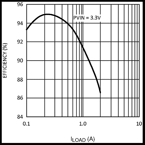
3.1 Efficiency vs ILOAD
