SNVS421H January 2006 – October 2017 LM3100
PRODUCTION DATA.
- 1 Features
- 2 Applications
- 3 Description
- 4 Revision History
- 5 Pin Configuration and Functions
- 6 Specifications
- 7 Detailed Description
- 8 Applications and Implementation
- 9 Layout
- 10Device and Documentation Support
- 11Mechanical, Packaging, and Orderable Information
Package Options
Mechanical Data (Package|Pins)
- PWP|20
Thermal pad, mechanical data (Package|Pins)
- PWP|20
Orderable Information
1 Features
- Input Voltage Range 4.5 V to 36 V
- 1.5 A Output Current
- 0.8 V, ±1.5% Reference
- Integrated 40 V, Dual N-Channel Buck Synchronous Switches
- Low Component Count and Small Solution Size
- No Loop Compensation Required
- Ultra-Fast Transient Response
- Stable With Ceramic and Other Low ESR Capacitors
- Programmable Switching Frequency up to 1 MHz
- Max. Duty Cycle Limited During Start-Up
- Valley Current Limit
- Precision Internal Reference for Adjustable Output Voltage Down to 0.8 V
- Thermal Shutdown
- Thermally Enhanced HTSSOP-20 Package
2 Applications
- 5VDC, 12VDC, 24VDC, 12VAC, and 24VAC Systems
- Embedded Systems
- Industrial Controls
- Automotive Telematics and Body Electronics
- Point of Load Regulators
- Storage Systems
- Broadband Infrastructure
- Direct Conversion from 2/3/4 Cell Lithium Batteries Systems
3 Description
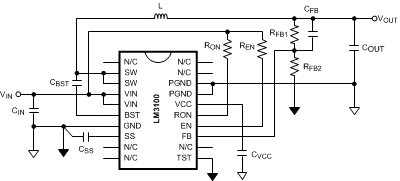
The LM3100 Synchronously Rectified Buck Converter features all functions needed to implement a highly efficient, cost effective buck regulator capable of supplying 1.5 A to loads with voltages as low as 0.8 V. Dual 40 V N-Channel synchronous MOSFET switches allow for low external component thus reducing complexity and minimizing board space. The LM3100 is designed to work exceptionally well with ceramic and other very low ESR output capacitors. The Constant ON-Time (COT) regulation scheme requires no loop compensation, results in fast load transient response, and simplifies circuit implementation. Through the use of a unique design the regulator does not rely on output capacitor ESR for stability, as do most other COT regulators. The operating frequency remains nearly constant with line and load variations due to the inverse relationship between the input voltage and the on-time. The operating frequency can be externally programmed up to 1 MHz. Protection features include VCC under-voltage lockout, thermal shutdown and gate drive under-voltage lockout. The part is available in a thermally enhanced HTSSOP-20 package
Device Information
| PART NUMBER | PACKAGE | BODY SIZE (NOM) |
|---|---|---|
| LM3100 | HTSSOP (20) | 6.50 mm × 4.40 mm |
- For all available packages, see the orderable addendum at the end of the data sheet.
Typical Application
