SNOSBI2C June 1999 – September 2015 LM231 , LM331
PRODUCTION DATA.
- 1 Features
- 2 Applications
- 3 Description
- 4 Revision History
- 5 Description continued
- 6 Pin Configuration and Functions
- 7 Specifications
- 8 Detailed Description
- 9 Application and Implementation
- 10Power Supply Recommendations
- 11Layout
- 12Device and Documentation Support
- 13Mechanical, Packaging, and Orderable Information
Package Options
Mechanical Data (Package|Pins)
- P|8
Thermal pad, mechanical data (Package|Pins)
Orderable Information
8 Detailed Description
8.1 Overview
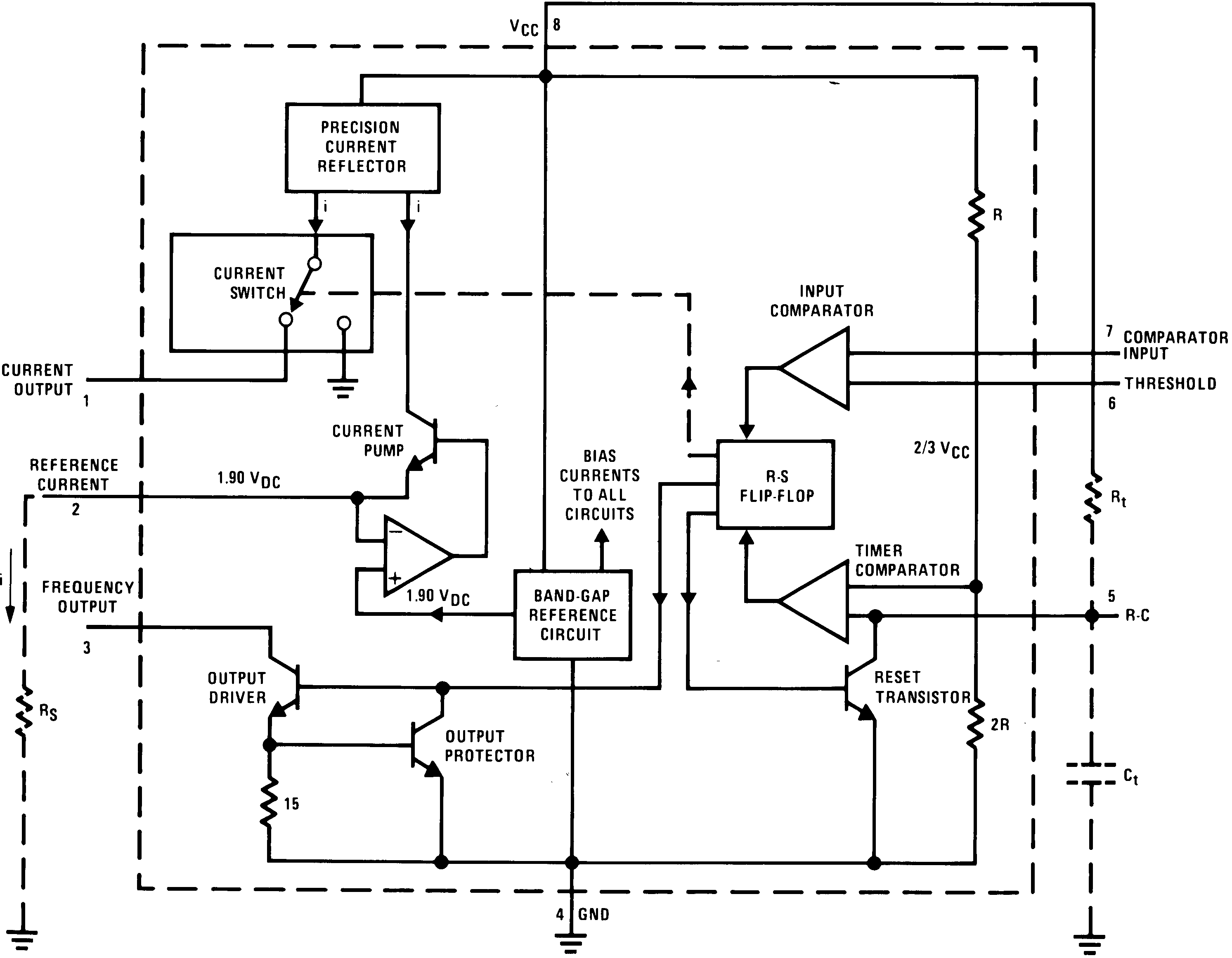
8.1.1 Detail of Operation, Functional Block Diagram
The Functional Block Diagram shows a band gap reference which provides a stable 1.9-VDC output. This 1.9 VDC is well regulated over a VS range of 3.9 V to 40 V. It also has a flat, low temperature coefficient, and typically changes less than ½% over a 100°C temperature change.
The current pump circuit forces the voltage at pin 2 to be at 1.9 V, and causes a current i = 1.90 V/RS to flow. For RS=14 k, i=135 μA. The precision current reflector provides a current equal to i to the current switch. The current switch switches the current to pin 1 or to ground, depending upon the state of the R-S flip-flop.
The timing function consists of an R-S flip-flop and a timer comparator connected to the external RtCt network. When the input comparator detects a voltage at pin 7 higher than pin 6, it sets the R-S flip-flop which turns ON the current switch and the output driver transistor. When the voltage at pin 5 rises to ⅔ VCC, the timer comparator causes the R-S flip-flop to reset. The reset transistor is then turned ON and the current switch is turned OFF.
However, if the input comparator still detects the voltage on pin 7 as higher than pin 6 when pin 5 crosses ⅔ VCC, the flip-flop will not be reset, and the current at pin 1 will continue to flow, trying to make the voltage at pin 6 higher than pin 7. This condition will usually apply under start-up conditions or in the case of an overload voltage at signal input. During this sort of overload the output frequency will be 0. As soon as the signal is restored to the working range, the output frequency will be resumed.
8.2 Functional Block Diagram

8.3 Feature Description
The LMx31 operate over a wide voltage range of 4 V to 40 V.
The voltage at pin 2 is regulated at 1.90 VDC for all values of i between 10 μA to 500 μA. It can be used as a voltage reference for other components, but take care to ensure that current is not taken from it which could reduce the accuracy of the converter.
8.4 Device Functional Modes
The output driver transistor acts to saturate pin 3 with an ON resistance of about 50 Ω. In case of overvoltage, the output current is actively limited to less than 50 mA.
If the voltage on pin 7 is higher than pin 6 when pin 5 crosses ⅔ VCC, the LMx31 internal flip-flop will not be reset, and the current at pin 1 will continue to flow, trying to make the voltage at pin 6 higher than pin 7. This condition will usually apply under start-up conditions or in the case of an overload voltage at signal input. During this sort of overload the output frequency will be 0. As soon as the signal is restored to the working range, the output frequency will be resumed.