SLVS047L November 1981 – January 2015 LM237 , LM337
PRODUCTION DATA.
- 1 Features
- 2 Applications
- 3 Description
- 4 Simplified Schematic
- 5 Revision History
- 6 Pin Configuration and Functions
- 7 Specifications
- 8 Detailed Description
- 9 Application and Implementation
- 10Power Supply Recommendations
- 11Layout
- 12Device and Documentation Support
- 13Mechanical, Packaging, and Orderable Information
Package Options
Mechanical Data (Package|Pins)
Thermal pad, mechanical data (Package|Pins)
Orderable Information
6 Pin Configuration and Functions
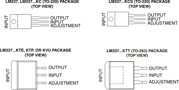
Pin Functions
| PIN | TYPE | DESCRIPTION | |
|---|---|---|---|
| NAME | NO. | ||
| ADJUSTMENT | 1 | I | Adjustment pin for the output voltage. Connect two external resistors to adjust the output voltage. |
| INPUT | 2 | I | Input voltage. The input voltage and current will be designated VI and II respectively. |
| OUTPUT | 3 | O | Output voltage. The output voltage and current will be designated VO and IO respectively. |