SNVS089O July 2000 – July 2015 LM3488
PRODUCTION DATA.
- 1 Features
- 2 Applications
- 3 Description
- 4 Revision History
- 5 Pin Configuration and Functions
- 6 Specifications
- 7 Detailed Description
-
8 Application and Implementation
- 8.1 Application Information
- 8.2
Typical Applications
- 8.2.1
Boost Converter
- 8.2.1.1 Design Requirements
- 8.2.1.2
Detailed Design Procedure
- 8.2.1.2.1 Custom Design with WEBENCH Tools
- 8.2.1.2.2 Power Inductor Selection
- 8.2.1.2.3 Programming the Output Voltage
- 8.2.1.2.4 Setting the Current Limit
- 8.2.1.2.5 Current Limit with External Slope Compensation
- 8.2.1.2.6 Power Diode Selection
- 8.2.1.2.7 Power MOSFET Selection
- 8.2.1.2.8 Input Capacitor Selection
- 8.2.1.2.9 Output Capacitor Selection
- 8.2.1.3 Application Curve
- 8.2.2 Designing SEPIC Using LM3488
- 8.2.1
Boost Converter
- 9 Power Supply Recommendations
- 10Layout
- 11Device and Documentation Support
- 12Mechanical, Packaging, and Orderable Information
Package Options
Mechanical Data (Package|Pins)
- DGK|8
Thermal pad, mechanical data (Package|Pins)
- DGK|8
Orderable Information
1 Features
- Automotive Grade Product, AEC-Q100 Qualified
- 8-Lead VSSOP Package
- Internal Push-Pull Driver With 1-A Peak Current Capability
- Current Limit and Thermal Shutdown
- Frequency Compensation Optimized With a Capacitor and a Resistor
- Internal Soft-Start
- Current Mode Operation
- Undervoltage Lockout With Hysteresis
- Key Specifications:
- Wide Supply Voltage Range of 2.97 V to 40 V
- 100-kHz to 1-MHz Adjustable and Synchronizable Clock Frequency
- ±1.5% (Overtemperature) Internal Reference
- 5-µA Shutdown Current (Overtemperature)
- Create a Custom Design Using the LM3488 with the WEBENCH Power Designer
2 Applications
3 Description
The LM3488 is a versatile low-side N-FET high-performance controller for switching regulators. This device is suitable for use in topologies requiring low-side FET, such as boost, flyback, or SEPIC. Moreover, the LM3488 can be operated at extremely high switching frequency to reduce the overall solution size. The switching frequency of LM3488 can be adjusted to any value from 100 kHz to 1 MHz by using a single external resistor or by synchronizing it to an external clock. Current mode control provides superior bandwidth and transient response, besides cycle-by-cycle current limiting. Output current can be programmed with a single external resistor.
The LM3488 has built-in features such as thermal shutdown, short-circuit protection, and overvoltage protection. Power-saving shutdown mode reduces the total supply current to 5 µA and allows power supply sequencing. Internal soft-start limits the inrush current at start-up.
Device Information(1)
| PART NUMBER | PACKAGE | BODY SIZE (NOM) |
|---|---|---|
| LM3488 | VSSOP (8) | 3.00 mm × 3.00 mm |
| LM3488-Q1 |
- For all available packages, see the orderable addendum at the end of the datasheet.
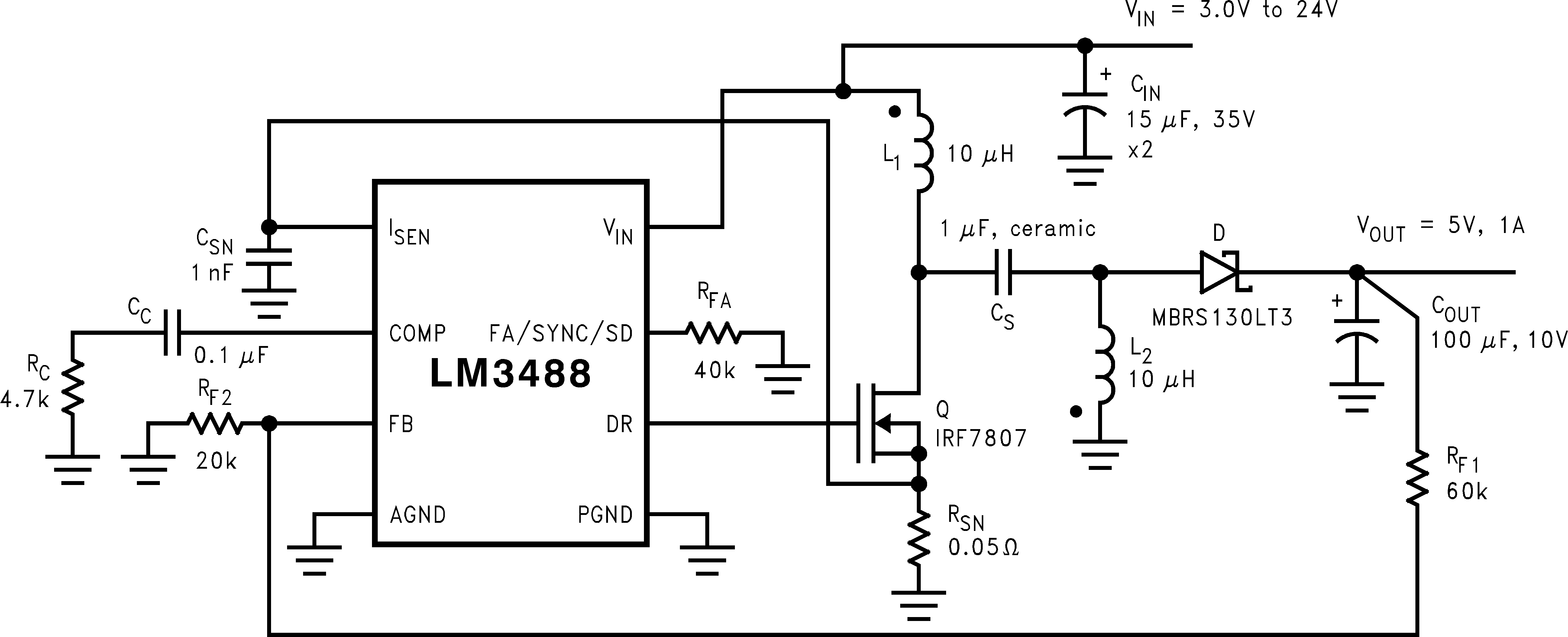
Typical SEPIC Converter
