SNVS443C May 2006 – December 2016 LM3489 , LM3489-Q1
PRODUCTION DATA.
- 1 Features
- 2 Applications
- 3 Description
- 4 Revision History
- 5 Pin Configuration and Functions
- 6 Specifications
- 7 Detailed Description
- 8 Application and Implementation
- 9 Power Supply Recommendations
- 10Layout
- 11Device and Documentation Support
- 12Mechanical, Packaging, and Orderable Information
Package Options
Mechanical Data (Package|Pins)
- DGK|8
Thermal pad, mechanical data (Package|Pins)
- DGK|8
Orderable Information
1 Features
- Qualified for Automotive Parts
- AEC-Q100 Qualified With the Following Results:
- Device Temperature Grade 1: –40°C to 125°C Ambient Operating Temperature Range
- Device HBM ESD Classification Level 2
- Device CDM ESD Classification Level C5
- Easy-to-Use Control Methodology
- No Control Loop Compensation Required
- Wide 4.5-V to 35-V Input Range
- 1.239 V to VIN Adjustable Output Range
- High Efficiency: 93%
- ±1.3% (±2% Over Temperature) Internal Reference
- 100% Duty Cycle Operation
- Maximum Operation Frequency > 1 MHz
- Current Limit Protection
- Dedicated Enable Pin (on if Unconnected)
- Shutdown Mode Draws Only 7-µA Supply Current
- 8-Pin VSSOP Package
2 Applications
- Set-Top Boxes
- DSL or Cable Modems
- PC/IA
- Auto PCs
- TFT Monitors
- Battery-Powered Portable Applications
- Distributed Power Systems
- Always-On Power
- High-Power LED Drivers
- Automotive
3 Description
The LM3489 device is a high-efficiency PFET switching regulator controller that can be used to quickly and easily develop a small, cost-effective, switching buck regulator for a wide range of applications. The hysteretic control architecture provides for simple design without any control loop stability concerns using a wide variety of external components. The PFET architecture also allows for low component count as well as ultra-low dropout, 100% duty cycle operation. Another benefit is high efficiency operation at light loads without an increase in output ripple. A dedicated enable pin provides a shutdown mode drawing only 7 µA. Leaving the enable pin unconnected defaults to on.
Current limit protection can be implemented by measuring the voltage across the PFET’s RDS(ON), thus eliminating the need for a sense resistor. A sense resistor may be used to improve current limit accuracy if desired. The cycle-by-cycle current limit can be adjusted with a single resistor, ensuring safe operation over a range of output currents.
Device Information(1)
| PART NUMBER | PACKAGE | BODY SIZE (NOM) |
|---|---|---|
| LM3489 LM3489-Q1 |
VSSOP (8) | 3.00 mm × 3.00 mm |
- For all available packages, see the orderable addendum at the end of the data sheet.
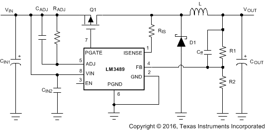
Typical Application Circuit
